36
Mohammad Mahdi Khafaji High Speed CurrentSteering DACs in SiGe BiCMOS Technology

Mohammad Mahdi Khafaji
High Speed CurrentSteering DACsin SiGe BiCMOS Technology

High Speed CurrentSteering DACsin SiGe BiCMOS Technology
Mohammad Mahdi Khafaji
Beiträge aus der Informationstechnik
Dresden 2015

Bibliografische Information der Deutschen NationalbibliothekDie Deutsche Nationalbibliothek verzeichnet diese Publikation in derDeutschen Nationalbibliografie; detaillierte bibliografische Daten sind imInternet über http://dnb.dnb.de abrufbar.
Bibliographic Information published by the Deutsche NationalbibliothekThe Deutsche Nationalbibliothek lists this publication in the DeutscheNationalbibliografie; detailed bibliographic data are available on theInternet at http://dnb.dnb.de.
Zugl.: Dresden, Techn. Univ., Diss., 2015
Die vorliegende Arbeit stimmt mit dem Original der Dissertation„High Speed CurrentSteering DACs in SiGe BiCMOS Technology“ vonMohammad Mahdi Khafaji überein.
© Jörg Vogt Verlag 2015Alle Rechte vorbehalten. All rights reserved.
Gesetzt vom Autor
ISBN 9783938860854
Jörg Vogt VerlagNiederwaldstr. 3601277 DresdenGermany
Phone: +49(0)35131403921Telefax: +49(0)35131403918email: [email protected] : www.vogtverlag.de
Technische Universität Dresden
HIGH SPEED CURRENT-STEERING DACS
IN SIGE BICMOS TECHNOLOGY
MOHAMMAD MAHDI KHAFAJI
der Fakultät Elektrotechnik und Informationstechnikder Technischen Universität Dresden
zur Erlangung des akademischen Grades
Doktoringenieur(Dr.-Ing.)
genehmigte Dissertation
Vorsitzender: Prof. Dr.-Ing. STEFFEN BERNET
Gutachter: Prof. Dr. sc. techn. habil. Dipl. Betriebswiss. FRANK ELLINGER
Prof. Dr.-Ing. CHRISTOPH SCHEYTT
Tag der Einreichung: 16. 6. 2014Tag der Verteidigung: 18. 2. 2015

Dedicated to Abul-Fadhl Al-Abbas, the one who taught me the way of life.
ABSTRACT
The evolution of communication systems has been the strongest motivationof the rapid improvement of data converters in recent years. In optical com-munications, utilizing spectrally-efficient modulation schemes was the mainkey to meet the demand of higher bit rates. This, however, required digital-to-analog converters (DACs) with 5-8 bit resolution at a sampling rate of tens ofGigahertz. In the frame of this work an attempt has been made to address thischallenge.
After a brief overview of current-steering DAC architectures, the static anddynamic sources of error are mentioned in chapter 2. At medium resolutions,achieving the required static performance is not a critical task in recent silicontechnology nodes. On the other hand, the dynamic DAC performance at veryhigh speeds is a different story. In chapter 3, we investigate the impact of thedynamic output impedance and the time response of current switches as deci-sive factors in understanding DAC high-frequency behaviour. It is shown that aDAC in a bipolar technology can potentially provide two more resolution bitscompared to an equivalent CMOS design.
To improve the characteristics of a current switch cell as the main bottleneckin designing current-steering DACs, a modified circuit is proposed in chapter4. Its static and dynamic characteristics are examined and compared with tho-se of a conventional design. A design strategy for better matching of rise (fall)times of different cells is presented. The input capacitor of the presented cellcan be lower than that of a cascode differential pair. At the same time, therise (fall) time mismatch are decreased by factor of two for a targeted 6-bitDAC. Based on this current switch, the 6-bit fully binary DAC with 28 GSpsin a SiGe 0.25 µm technology is demonstrated. The measurement results showsuitable functionality of this component in a recent 100 Gbps optical transmit-
VII
ter. This design has the best figure-of-merit of binary DACs in a silicon-basedtechnology.
Chapter 5 presents a way of generating synchronous bit streams to test aDAC at its full speed. The proposed system is composed of several multiplexerswith built-in memory cells. Those multiplexers have to be synchronized bya resettable and also adjustable clock signal. Using a hierarchical top-downmethod, all the blocks and sub-blocks of the complete system are explained.The measurements of the memory-multiplexer chip as well as clock generatorchip are presented. The implemented system in a SiGe 0.25 µm technology iscapable of supplying the needed bit stream at 28 GSps.
VIII
ZUSAMMENFASSUNG
Die größte Motivation für die drastische Verbesserung von Datenwandlern inden letzten Jahren war die stetige Verbesserung der Kommunikationssysteme.In optischen Kommunikationssystemen konnten durch die Verwendung vonModulationsverfahren mit hoher spektraler Effizienz größere Datenraten er-zielt werden. Hierzu wurden jedoch Digital-Analog-Wandler (digital-to-analogconverters, DACs) mit fünf bis acht Bit Auflösung bei Samplingraten von meh-reren zehn Gigahertz benötigt. Diese Arbeit beschäftigt sich mit den Heraus-forderungen des Entwurfs derartiger DACs.
Nach einem kurzen Überblick über stromgesteuerte DACs werden in Kapi-tel 2 deren statische und dynamische Fehlerquellen untersucht. Das geforder-te statische Verhalten eines DACs mit mittlerer Auflösung kann in modernenHalbleitertechnologien problemlos erreicht werden. Für das dynamische Ver-halten bei hohen Frequenzen trifft diese Aussage jedoch nicht zu. In Kapitel 3wird gezeigt, dass die dynamische Ausgangsimpedanz und das zeitliche Ver-halten von geschalteten Stromquellen maßgebliche Faktoren für die Funktionvon DACs bei hohen Frequenzen darstellen. Es wird gezeigt, dass die Auflö-sung von DACs mit Bipolar-Transistoren um bis zu zwei Bit höher sein kannals die von CMOS-DACs.
Um die Eigenschaften einer geschalteten Stromquelle als maßgeblich limi-tieren Faktor im Entwurf von stromgesteuerten DACs zu verbessern, wird inKapitel 4 eine veränderte Schaltung vorgestellt. Deren statische und dynami-sche Eigenschaften werden untersucht und mit denen eines konventionellenEntwurfs verglichen. Dabei wird eine Entwurfsmethodik für eine verbesser-te Übereinstimmung von Anstiegs-/Abfallzeiten verschiedener Zellen vorge-stellt. Die Eingangskapazität der vorgestellten Zelle kann geringer sein als dieeines differentiellen Kaskode-Paares. Gleichzeitig werden die Abweichungen
IX

in der Anstiegs-/Abfallzeit für einen geplanten vollständig binären 6 Bit DACum den Faktor 2 reduziert. Basierend auf dieser geschalteten Stromquelle wirdein 6 Bit DAC mit 28 Gbit/s in einer SiGe 0.25 µm Technologie demonstriert.Die Messergebnisse zeigen eine geeignete Funktionalität dieser Komponentein einem modernen optischen 100 Gbit/s Sender. Dieser Entwurf weist den be-sten Bewertungsfaktor (Figure of Merit, FoM) binärer DACs in einer silizium-basierten Technology auf.
In Kaptiel 5 wird eine Methode zur Generierung von synchronen Bitströ-men beschrieben, um einen DAC bei seiner vollen Geschwindigkeit testenzu können. Das resultierende System besteht aus mehreren Multiplexern miteingebauten Speicherzellen. Diese Multiplexer müssen mittels eines zurück-setzbaren und anpassbaren Taktsignals synchronisiert werden. Alle Elementedes Gesamtsystems werden durch Nutzung der top-down-Methode beschrie-ben und analysiert. Anschließend werden die Messergebnisse präsentiert. Dasin einer SiGe 0.25µm Technology implementierte System kann zur Versorgungeines Bitstromes bei 28 GSps genutzt werden.
X

ACKNOWLEDGEMENTS
First and foremost, I would like to thank God for all the blessing over theentire duration of this work and my life.
I would like to express the highest appreciation to both of my supervisors,professor Frank Ellinger, whose scientific insight has always been motivat-ing and professor Christoph Scheytt who was providing an ingenious solutionfor each problem I encountered. Their suggestions, encouragement, and com-ments were invaluable to me. I owe a very important debt to Dr. Hans Gustatwhose personality and creativity was ever inspiring. He was my supervisor fortwo and half years in IHP Microelectronics, and he has been extraordinarilytolerant and supportive. I will benefit from his advices lifelong. Without thepersistent support of IHP Microelectronics GmbH this dissertation would nothave been possible. I am grateful to them. In addition, I would particularly liketo acknowledge the help of professor Udo Jörges whose meticulous commentswere greatly insightful.
It gives me great pleasure in expressing my gratitude to Dr. Behnam Sedighi,a friend who by his own analytical way of thinking gave me lots of constructivecomments. I have also greatly benefited from Dr. Corrado Carta, my supervisorin the last two years, whose office was always open when I had a question andmade immense contribution to the writing.
I have learned a lot from discussions with Jian Zhu, Ahmed Awny, GregorTretter, and Mohamed Elkhouly. It was a joy to have such colleagues and Iwould like to offer my special thanks to them. The presented work in the lastdesign chapter could not be materialized without the help and persistence ofDr. Klaus Tittelbach-Helmrich, Dr. Daniel Micusik, Dr. Gunter Fischer, andVladimir Petrovic. I am indebted to my many colleagues who supported meduring all those years, among them I would particularly like to thank Dr. Frank
XI

Herzel, Carmelo Nicita, Jan Wessel, Neelanjan Sharmah, David Fritsche, JanDirk Leufker, Maruf Hossain, Dave Stolarek, Arzu Ergintav, Jörg Klatt, DenysMartynenko, and Dinesh Venkitachalam.
During stressful measurements I received generous assistance from FrankPopiela, Dr. Stefan Schumann, Robert Wolf, Dr. Yevgen Borokhovych, Dr.Sabbir Osmany, and Johannes Borngräber. I received extraordinary supportfrom Bernhard Schweiger at Agilent Technologies who made it possible tomeasure the presented digital to analog converter in the thesis.
The last but not the least people to mention are the most important ones inmy life, my family. The accomplishment of this work would not be possiblewithout them. My parents, brother, and sisters are the great source of encour-agement to my life. I cannot adequately express the love and gratitude I feelfor them. In particular I must acknowledge my wife, my best friend, withoutwhose love, support, patience, and assistance I would not have finished thiswork.Dresden, February 2015 Mohammad Mahdi Khafaji
XII
CONTENTS
1 Introduction 11.1 Motivation . . . . . . . . . . . . . . . . . . . . . . . . . . . . 11.2 Thesis Organization . . . . . . . . . . . . . . . . . . . . . . . 2
2 An Overview of Current-Steering DAC Structures 52.1 Introduction . . . . . . . . . . . . . . . . . . . . . . . . . . . 52.2 Current-Steering DAC Architectures . . . . . . . . . . . . . . 5
2.2.1 Binary Weighted DAC . . . . . . . . . . . . . . . . . 52.2.2 R-2R Ladder DAC . . . . . . . . . . . . . . . . . . . 72.2.3 Unary Weighted DAC . . . . . . . . . . . . . . . . . 82.2.4 Segmented DAC . . . . . . . . . . . . . . . . . . . . 10
2.3 Error Sources in Current-Steering DACs . . . . . . . . . . . . 112.3.1 Static Error Sources . . . . . . . . . . . . . . . . . . 122.3.2 Dynamic Error Sources . . . . . . . . . . . . . . . . . 15
2.4 Conclusion . . . . . . . . . . . . . . . . . . . . . . . . . . . 15
3 SFDR Considerations in Current Steering DACs 173.1 Introduction . . . . . . . . . . . . . . . . . . . . . . . . . . . 173.2 Rise(Fall) Time Mismatch Effect in High-Speed DACs . . . . 19
3.2.1 System Level Model . . . . . . . . . . . . . . . . . . 203.2.2 Simulation Results and Discussion . . . . . . . . . . . 223.2.3 Conclusion . . . . . . . . . . . . . . . . . . . . . . . 25
3.3 Output Impedance and Distortion Calculation . . . . . . . . . 263.3.1 Non-Ideal Switch Effect at Low Frequencies . . . . . 273.3.2 Switching of the Capacitive Load . . . . . . . . . . . 30
XIII
Contents
3.4 Device Metrics Effect on the DAC SFDR . . . . . . . . . . . 343.4.1 Basic Switch . . . . . . . . . . . . . . . . . . . . . . 343.4.2 Cascode Switch . . . . . . . . . . . . . . . . . . . . . 37
3.5 Discussion . . . . . . . . . . . . . . . . . . . . . . . . . . . . 393.5.1 Conclusions . . . . . . . . . . . . . . . . . . . . . . . 42
4 A 6-bit 28-GSps Binary DAC Design 434.1 Introduction . . . . . . . . . . . . . . . . . . . . . . . . . . . 434.2 Emitter-Coupled Logic and Emitter-Followers . . . . . . . . . 44
4.2.1 Bipolar Transistor Current Gain . . . . . . . . . . . . 444.2.2 The Conversion of Impedances . . . . . . . . . . . . . 45
4.3 Slew Rate in Binary-Weighted Current Switch Cells . . . . . . 494.4 Proposed Current Switch Cell . . . . . . . . . . . . . . . . . 54
4.4.1 Circuit Description and Basic Operation . . . . . . . . 554.4.2 Secondary Effects . . . . . . . . . . . . . . . . . . . 574.4.3 Mismatch Effects . . . . . . . . . . . . . . . . . . . . 584.4.4 Input Capacitance and Slew Rate . . . . . . . . . . . 594.4.5 High Current Density and Transit Frequency . . . . . 634.4.6 Small Signal Analysis . . . . . . . . . . . . . . . . . 64
4.5 6-bit DAC Implementation . . . . . . . . . . . . . . . . . . . 674.5.1 Current Switch Design . . . . . . . . . . . . . . . . . 684.5.2 Input Stage . . . . . . . . . . . . . . . . . . . . . . . 714.5.3 Clock Driver . . . . . . . . . . . . . . . . . . . . . . 734.5.4 Output Drivers and Output Network . . . . . . . . . . 74
4.6 Measurement and Results . . . . . . . . . . . . . . . . . . . . 754.6.1 Measurement Setup . . . . . . . . . . . . . . . . . . . 754.6.2 Results . . . . . . . . . . . . . . . . . . . . . . . . . 764.6.3 Comparison with Other Published DACs . . . . . . . 80
4.7 Conclusion . . . . . . . . . . . . . . . . . . . . . . . . . . . 80
5 An 8-bit 28-GSps Arbitrary Signal Generator for Testing DACs 835.1 Introduction . . . . . . . . . . . . . . . . . . . . . . . . . . . 835.2 System Level Architecture . . . . . . . . . . . . . . . . . . . 84
XIV
Contents
5.3 MUX-Memory Chip . . . . . . . . . . . . . . . . . . . . . . 855.3.1 ECL/CML MUX . . . . . . . . . . . . . . . . . . . . 86
5.4 Clock Generator Chip . . . . . . . . . . . . . . . . . . . . . . 935.5 Circuit Design . . . . . . . . . . . . . . . . . . . . . . . . . . 95
5.5.1 Latch Design . . . . . . . . . . . . . . . . . . . . . . 955.5.2 Biasing . . . . . . . . . . . . . . . . . . . . . . . . . 975.5.3 2:1 MUX and One-Stage 4:1 MUX . . . . . . . . . . 975.5.4 Clock Driver . . . . . . . . . . . . . . . . . . . . . . 995.5.5 Input and Output Stage . . . . . . . . . . . . . . . . . 1015.5.6 Level Translators . . . . . . . . . . . . . . . . . . . . 1035.5.7 Phase Interpolator (PI) . . . . . . . . . . . . . . . . . 1045.5.8 28 GHz Clock Tree . . . . . . . . . . . . . . . . . . . 106
5.6 Measurement Results . . . . . . . . . . . . . . . . . . . . . . 1075.6.1 MUX . . . . . . . . . . . . . . . . . . . . . . . . . . 1075.6.2 Clock Generator . . . . . . . . . . . . . . . . . . . . 111
5.7 Conclusion . . . . . . . . . . . . . . . . . . . . . . . . . . . 112
6 Summary and Future Work 1156.1 Summary . . . . . . . . . . . . . . . . . . . . . . . . . . . . 1156.2 Future Work . . . . . . . . . . . . . . . . . . . . . . . . . . . 116
XV

XVI
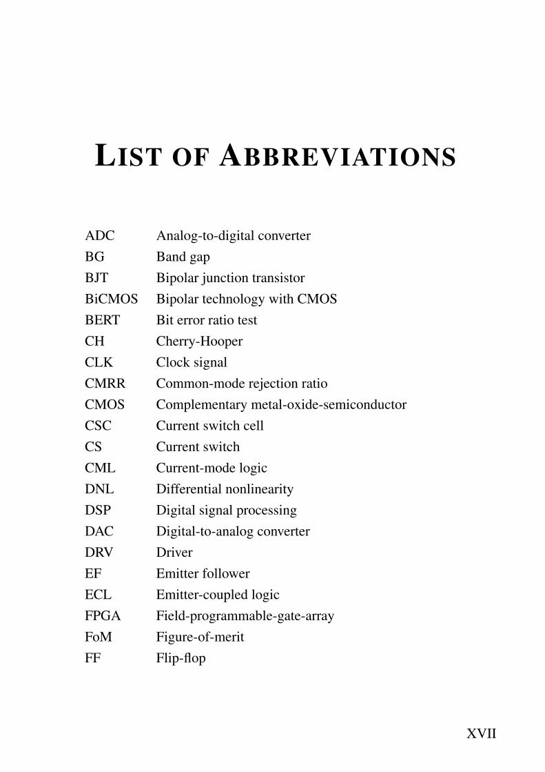
LIST OF ABBREVIATIONS
ADC Analog-to-digital converterBG Band gapBJT Bipolar junction transistorBiCMOS Bipolar technology with CMOSBERT Bit error ratio testCH Cherry-HooperCLK Clock signalCMRR Common-mode rejection ratioCMOS Complementary metal-oxide-semiconductorCSC Current switch cellCS Current switchCML Current-mode logicDNL Differential nonlinearityDSP Digital signal processingDAC Digital-to-analog converterDRV DriverEF Emitter followerECL Emitter-coupled logicFPGA Field-programmable-gate-arrayFoM Figure-of-meritFF Flip-flop
XVII
list of abbreviations
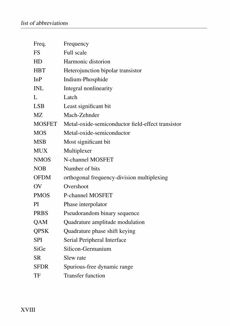
Freq. FrequencyFS Full scaleHD Harmonic distorionHBT Heterojunction bipolar transistorInP Indium-PhosphideINL Integral nonlinearityL LatchLSB Least significant bitMZ Mach-ZehnderMOSFET Metal-oxide-semiconductor field-effect transistorMOS Metal-oxide-semiconductorMSB Most significant bitMUX MultiplexerNMOS N-channel MOSFETNOB Number of bitsOFDM orthogonal frequency-division multiplexingOV OvershootPMOS P-channel MOSFETPI Phase interpolatorPRBS Pseudorandom binary sequenceQAM Quadrature amplitude modulationQPSK Quadrature phase shift keyingSPI Serial Peripheral InterfaceSiGe Silicon-GermaniumSR Slew rateSFDR Spurious-free dynamic rangeTF Transfer function
XVIII
LIST OF SYMBOLS
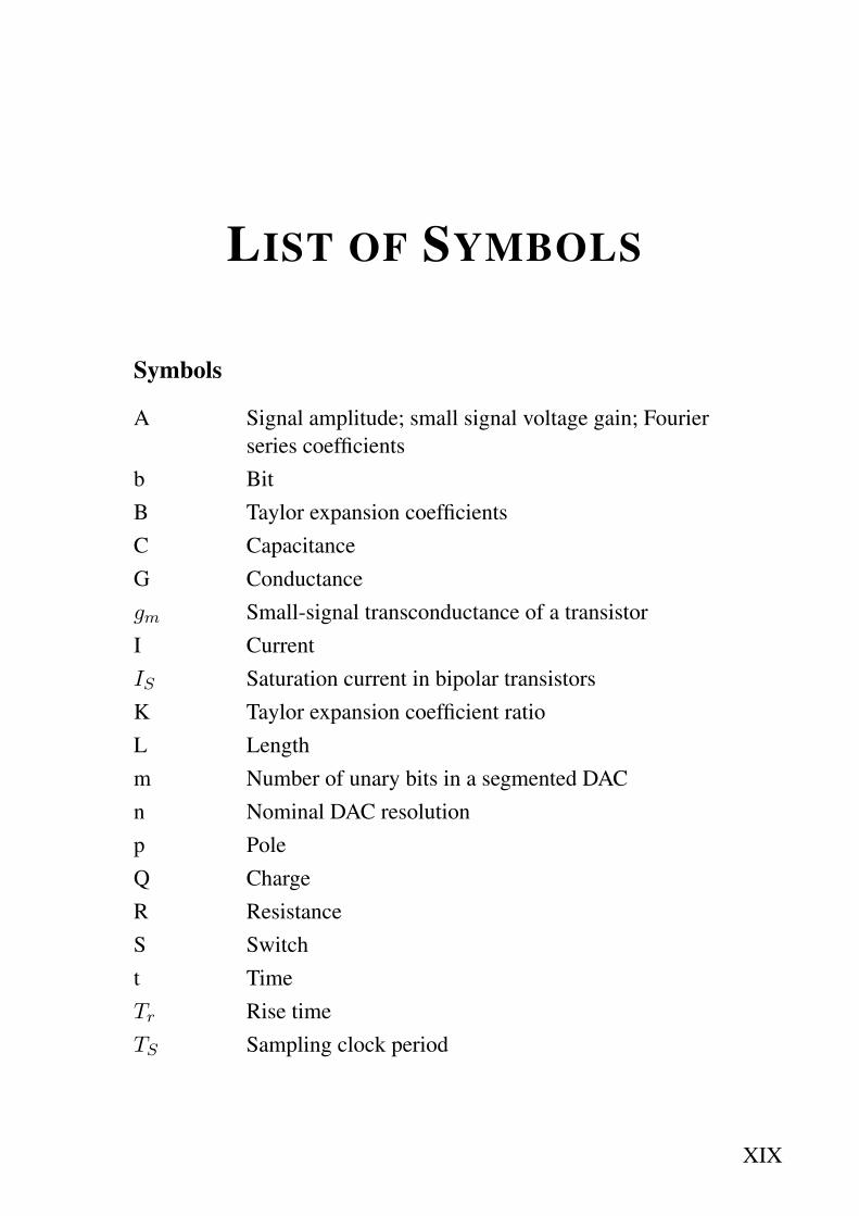
Symbols
A Signal amplitude; small signal voltage gain; Fourierseries coefficients
b BitB Taylor expansion coefficientsC CapacitanceG Conductancegm Small-signal transconductance of a transistorI CurrentIS Saturation current in bipolar transistorsK Taylor expansion coefficient ratioL Lengthm Number of unary bits in a segmented DACn Nominal DAC resolutionp PoleQ ChargeR ResistanceS Switcht TimeTr Rise timeTS Sampling clock period
XIX
list of symbols
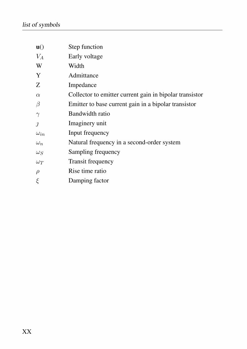
u() Step functionVA Early voltageW WidthY AdmittanceZ Impedanceα Collector to emitter current gain in bipolar transistorβ Emitter to base current gain in a bipolar transistorγ Bandwidth ratio Imaginery unitωin Input frequencyωn Natural frequency in a second-order systemωS Sampling frequencyωT Transit frequencyρ Rise time ratioξ Damping factor
XX
CHAPTER 1
INTRODUCTION
1.1 Motivation
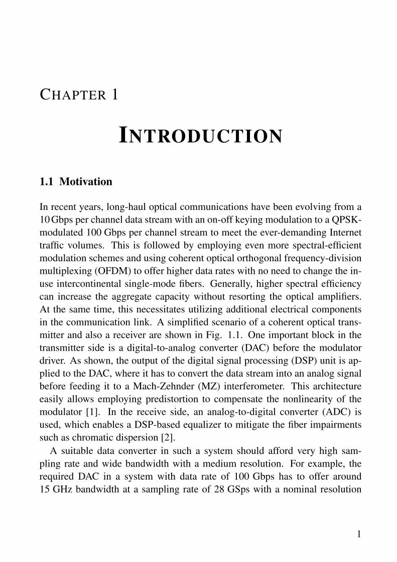
In recent years, long-haul optical communications have been evolving from a10 Gbps per channel data stream with an on-off keying modulation to a QPSK-modulated 100 Gbps per channel stream to meet the ever-demanding Internettraffic volumes. This is followed by employing even more spectral-efficientmodulation schemes and using coherent optical orthogonal frequency-divisionmultiplexing (OFDM) to offer higher data rates with no need to change the in-use intercontinental single-mode fibers. Generally, higher spectral efficiencycan increase the aggregate capacity without resorting the optical amplifiers.At the same time, this necessitates utilizing additional electrical componentsin the communication link. A simplified scenario of a coherent optical trans-mitter and also a receiver are shown in Fig. 1.1. One important block in thetransmitter side is a digital-to-analog converter (DAC) before the modulatordriver. As shown, the output of the digital signal processing (DSP) unit is ap-plied to the DAC, where it has to convert the data stream into an analog signalbefore feeding it to a Mach-Zehnder (MZ) interferometer. This architectureeasily allows employing predistortion to compensate the nonlinearity of themodulator [1]. In the receive side, an analog-to-digital converter (ADC) isused, which enables a DSP-based equalizer to mitigate the fiber impairmentssuch as chromatic dispersion [2].
A suitable data converter in such a system should afford very high sam-pling rate and wide bandwidth with a medium resolution. For example, therequired DAC in a system with data rate of 100 Gbps has to offer around15 GHz bandwidth at a sampling rate of 28 GSps with a nominal resolution
1

1 Introduction
DSP DAC
Mach-Zehnder
Modulator
LaserFiber
Driver
(a)
DSPADC
Photo Detector
FiberHybrid
TIA
Laser
(b)
Figure 1.1: A simplified coherent optical transmission system used in recent 100 Gbps commu-nications (a) the transmitter, and (b) the receiver. Notice the usage of data convertersin the link, which is a major change compared to the previous generation of on-offkeying based transmission.
of 6-bit [3] – [6]. At an output frequency close to its Nyquist rate, the DACshould still provide better than 4-bit resolution [5]. This is normally measuredin terms of spurious-free dynamic range (SFDR) and can be correlated to thehigh-frequency behaviour of the DAC.
1.2 Thesis Organization
The aim of this work is to study and investigate the challenges associated withdesigning and measuring DACs suitable for the recent optical systems. In thisregard, a brief introduction to current-steering DACs which are often used for
2
1.2 Thesis Organization
high-speed realizations is given in Chapter 2. There are many factors affect-ing the high-frequency behaviour of DACs. In Chapter 3, the delay amongdifferent bits as well as the impact of the output impedance are theoreticallyinvestigated. A modified current switching cell is presented in Chapter 4. Italso includes an implementation of a 6-bit DAC based on this current cell. Thedesigned DAC measurements are presented as well. To deal with the challengeof measuring high-speed DACs a simple method is chosen and the realiza-tion of the needed blocks is presented in chapter 5. In this approach severalsynchronized multiplexers with built-in memory cells generate the required bitstream. In chapter 6 the work is concluded and future remarks are presented.
The utilized technology allover this thesis is the BiCMOS SG25H1 0.25-µm technology of IHP [7]. It offers transistors with 180 GHz and 220 GHz asmaximum transit and oscillation frequency, respectively. Passive componentsand 5 metalization layers are available in this process, in which the topmost twometal layers have thickness of 3 µm and 2 µm and can be used to implementlow loss microwave structures.
3

4
CHAPTER 2
AN OVERVIEW OFCURRENT-STEERING DAC
STRUCTURES
2.1 Introduction
Among several methods of implementing a DAC, the most versatile one toachieve the highest rate functionality in a given process is the current-steeringapproach. As the name suggests, it is based on varying the direction of flowingcurrents to the output node. By means of digitally-controlled current switchesand summing the switched current at one point, it is possible to construct ananalog output corresponding to the input code. The output current can be con-verted to a voltage, e.g. by utilizing a resistor. There are widely used archi-tectures to realize such a DAC which are briefly discussed in this chapter. Thebenefits and drawbacks of each method are summarized and the bottlenecks inthe design are noted as well.
2.2 Current-Steering DAC Architectures
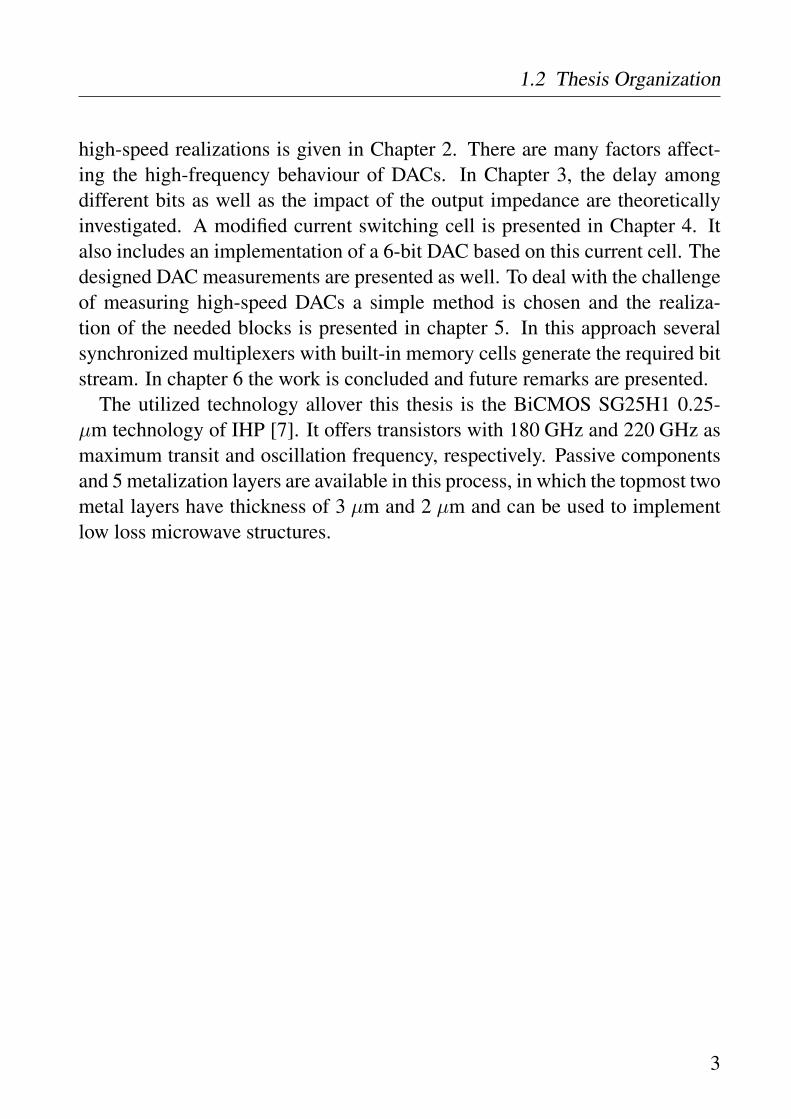
2.2.1 Binary Weighted DAC
At its simplest form, a current-steering DAC with n-bit resolution and inputbits of bn−1bn−2 . . . b0, can be implemented by n current switches, in whichthe currents are binary weighted, accordingly. This means that a targeted DACcan be realized with a minimum power and area. A conceptual view of the
5
2 An Overview of Current-Steering DAC Structures
VCC
IL
bn-1
VOUT
2n-1xILSB
bn-2
2n-2xILSB
b1
2xILSB
b0
ILSB
RL
Binary input
Figure 2.1: A conceptual diagram of a fully binary current-steering DAC. Matching among verydifferent current sources is one of the design challenges.
fully binary architecture is presented in Fig. 2.1. The least significant bit b0 iscontrolling a switch with the smallest current ILSB and so each bit is connectedto a switch according to its weight. The output current can be written as
IL = ILSB ×(b0 + 2b1 + · · · + 2n−2bn−2 + 2n−1bn−1
). (2.1)
While this is a very straight-forward implementation, its simplicity comes withmajor drawbacks. The first problem is related to the matching of the currentswitches. The accuracy of the output current of a DAC in a static conditionshould be better than ILSB; which means the largest current source shouldmatch a current 2n−1 times smaller. For example, in a 10-bit DAC, the mostsignificant bit should have a matching better than 0.2%. Achieving the re-quired matching factors requires special layout techniques and large areas forimplementation. If the current error becomes more than ILSB , the output is no
6
2.2 Current-Steering DAC Architectures
longer monotonic1. Such an input-output characteristic deviates the frequencydomain behaviour of the DAC and produces harmonics of the sinusoidal inputsignal at its output.
The other issue is related to the difference of switching behavior among thebits; which is resulted from the non-similar switches in this structure. Theswitching time may vary from one bit to another causing a wrong output for avery short time. At the midscale transition where the input code changes from011. . . 1 to 100. . . 0, the MSB switch is turned on and all the rest are turnedoff. If the time required to switch the MSB is more than that of turning offthe rest, there is an instant that the DAC output goes to 00. . . 0. It actuallyshows a glitch with half the total swing of the DAC when the input increasedby only one LSB. Glitches with lower amplitudes also happen at one-forth andone-eighth of the scale. This output behaviour generates harmonic distortionand severely degrades the frequency-domain performance.
2.2.2 R-2R Ladder DAC
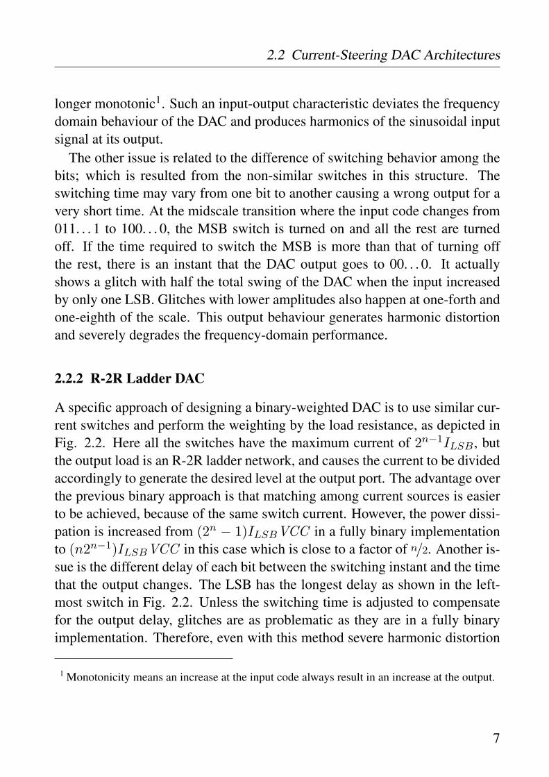
A specific approach of designing a binary-weighted DAC is to use similar cur-rent switches and perform the weighting by the load resistance, as depicted inFig. 2.2. Here all the switches have the maximum current of 2n−1ILSB , butthe output load is an R-2R ladder network, and causes the current to be dividedaccordingly to generate the desired level at the output port. The advantage overthe previous binary approach is that matching among current sources is easierto be achieved, because of the same switch current. However, the power dissi-pation is increased from (2n − 1)ILSBVCC in a fully binary implementationto (n2n−1)ILSBVCC in this case which is close to a factor of n/2. Another is-sue is the different delay of each bit between the switching instant and the timethat the output changes. The LSB has the longest delay as shown in the left-most switch in Fig. 2.2. Unless the switching time is adjusted to compensatefor the output delay, glitches are as problematic as they are in a fully binaryimplementation. Therefore, even with this method severe harmonic distortion
1 Monotonicity means an increase at the input code always result in an increase at the output.
7
2 An Overview of Current-Steering DAC Structures
VCC
VOUT
2RL
Binary input
2RL2RL
RL
2RL
RL
RL
RLRL
b0
2n-1xILSB
bn-2
2n-1xILSB
bn-1
2n-1xILSB
Figure 2.2: A simplified diagram of an R-2R current-steering DAC. All the current sources areequal and as large as the MSB one.
can be expected.Another consideration for high-speed applications is that the output network
consist of many resistors which have to be matched together. For each extrabit of resolution, the area of all the resistors has to be accordingly increased.It causes the parasitics associated with those resistors to be scaled-up and limitthe bandwidth at the output. This makes employing the R-2R structure to bevery challenging for GHz-range design with more than 4-bit resolution in asilicon-based technology.
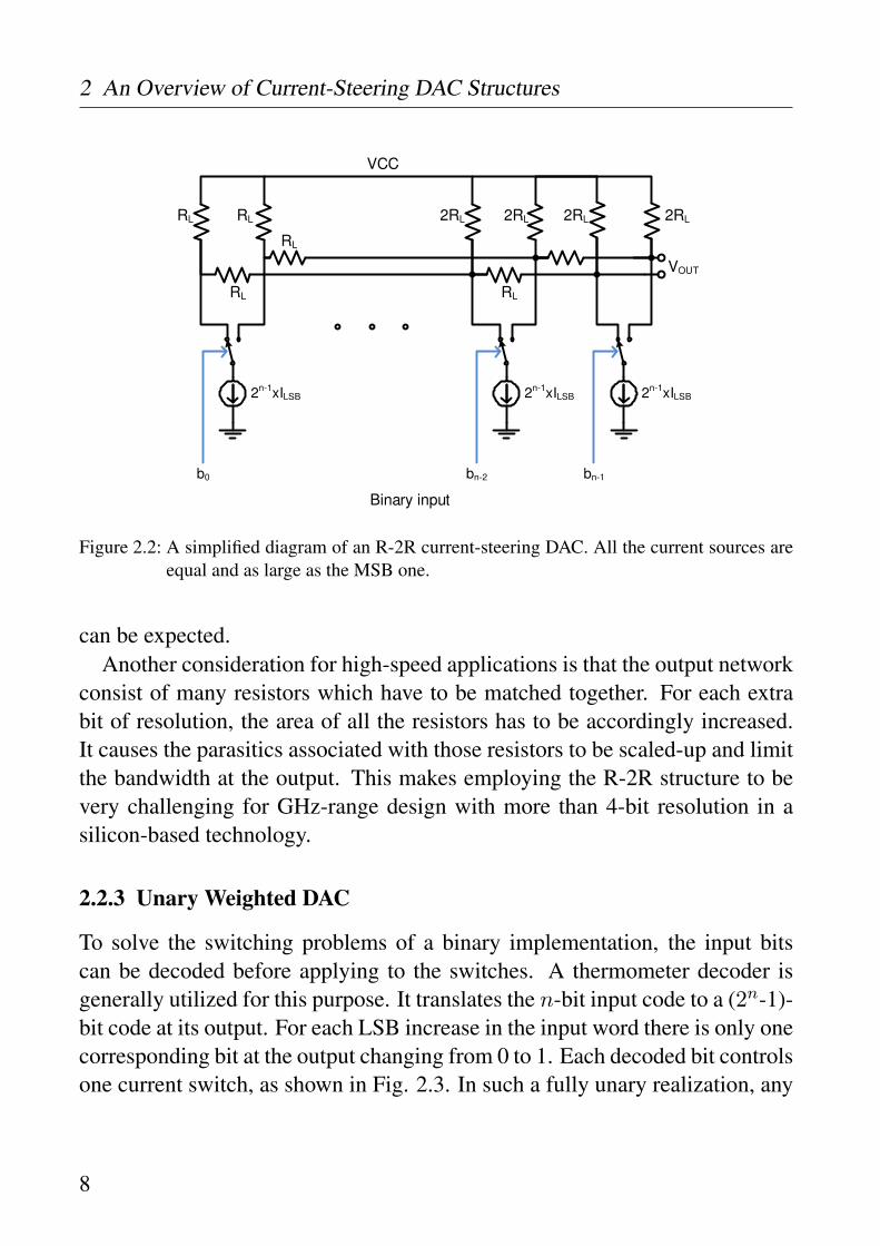
2.2.3 Unary Weighted DAC
To solve the switching problems of a binary implementation, the input bitscan be decoded before applying to the switches. A thermometer decoder isgenerally utilized for this purpose. It translates the n-bit input code to a (2n-1)-bit code at its output. For each LSB increase in the input word there is only onecorresponding bit at the output changing from 0 to 1. Each decoded bit controlsone current switch, as shown in Fig. 2.3. In such a fully unary realization, any
8
2.2 Current-Steering DAC Architectures
VCC
IL
bn-1
VOUT
ILSB
bn-2
ILSB
b1
ILSB
b0
ILSB
RL
Synchronizer (Flip-Flops)
Binary input
Binary to thermometer decoder
S1S2S2n-2S2
n-1
Figure 2.3: A simplified diagram of a fully unary current-steering DAC. The thermometer de-coder is implemented by combinational logics and so the latency of different outputsmay not be the same. The synchronization block ensures identical switching instantfor all the decoded bits.
increase or decrease at the input code causes some of the switches to be turnedon or off, respectively; but not both. Therefore, monotonicity of the DAC isguaranteed. At the same time using identical switches provides a matchingeasier than a fully binary approach. While the strength in this architecture isgiven by employing the decoder, it is the bottleneck of the system at the sametime.
The growth of the decoder is exponential and so is its area, interconnection,and power. By adding one bit to the DAC resolution, the area and the powerrequired for the DAC is doubled as well. At the same time, the complexityof the decoder is doubled. At high-speed designs, synchronization of switches
9
2 An Overview of Current-Steering DAC Structures
VCC
IL
bn-1
VOUT
bn-m bn-m-1 b0
ILSB
RL
Synchronizer (Flip-Flops)
Binary input
Binary to thermometer decoder
S1S2m
-1
2n-m-1xILSB
Delay equalizer
bn-m-1 b0
2n-m-1xILSB
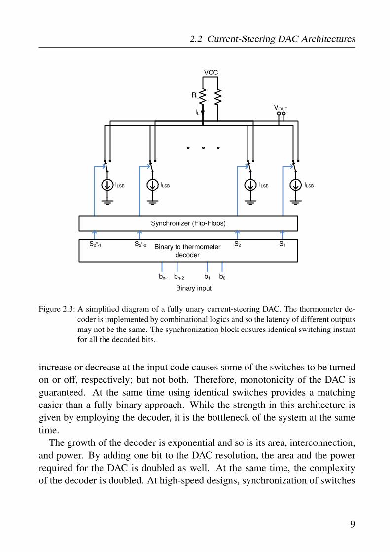
Figure 2.4: A simplified diagram of a segmented current-steering DAC implementation. Thehigher m significant bits are applied to the thermometer decoder. To compensate thelatency of the decoder, a delay equalizer has to be employed for the other (n − m)bits. All the bits have to be re-timed by the synchronizer block.
and routing become very challenging as well. It is very difficult to realize afully unary DAC with over 8-bit resolution up to now.
2.2.4 Segmented DAC
The segmented implementation is actually a compromise between the simplic-ity of the binary approach and the superior performance of the unary imple-mentation. A simplified block diagram is presented in Fig. 2.4. Here, thehigher m significant bits bn−1 . . . bn−m are applied to a thermometer decoderfor a unary realization. The other n − m bits bn−m−1 . . . b0 form the binary
10
2.3 Error Sources in Current-Steering DACs
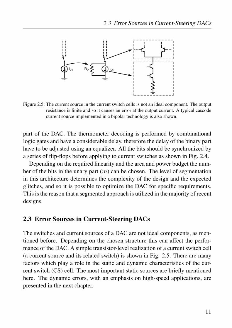
ICS ICSRO
Figure 2.5: The current source in the current switch cells is not an ideal component. The outputresistance is finite and so it causes an error at the output current. A typical cascodecurrent source implemented in a bipolar technology is also shown.
part of the DAC. The thermometer decoding is performed by combinationallogic gates and have a considerable delay, therefore the delay of the binary parthave to be adjusted using an equalizer. All the bits should be synchronized bya series of flip-flops before applying to current switches as shown in Fig. 2.4.
Depending on the required linearity and the area and power budget the num-ber of the bits in the unary part (m) can be chosen. The level of segmentationin this architecture determines the complexity of the design and the expectedglitches, and so it is possible to optimize the DAC for specific requirements.This is the reason that a segmented approach is utilized in the majority of recentdesigns.
2.3 Error Sources in Current-Steering DACs
The switches and current sources of a DAC are not ideal components, as men-tioned before. Depending on the chosen structure this can affect the perfor-mance of the DAC. A simple transistor-level realization of a current switch cell(a current source and its related switch) is shown in Fig. 2.5. There are manyfactors which play a role in the static and dynamic characteristics of the cur-rent switch (CS) cell. The most important static sources are briefly mentionedhere. The dynamic errors, with an emphasis on high-speed applications, arepresented in the next chapter.
11

2 An Overview of Current-Steering DAC Structures
2.3.1 Static Error Sources
In an ideal DAC, 1 LSB change in the digital input code corresponds to an out-put level change of 1 LSB; a voltage change of RLILSB in a current-steeringDAC. The deviation from the ideal output is commonly measured by differ-ential nonlinearity (DNL) and integral nonlinearity (INL). The DNL error isdefined as the deviation of the output level change from one LSB for everytwo succeeding input codes in the entire range. The INL error is defined as thedeviation of each output level from its ideal value. A maximum DNL of lessthan 1 LSB guarantees the monotonicity of the DAC. The DNL and INL aredirectly related to each other. The INL of the input code k can be obtained byknowing the DNL of all the input codes less than k, as follows:
INL(k) =k∑
i=1DNL(i). (2.2)
As the names suggest, both the INL and DNL are dealing with linearity ofa DAC, and they show its ability to reproduce the input code. The linearity ofa DAC has a direct impact on the dynamic behaviour as well, like generatingharmonic distortion at the output. Two important sources affecting the staticaccuracy of a DAC are the output impedance of the current source and processvariation.
As shown in Fig. 2.5, a current source has a finite output resistance (RO)which prevents the total current generated by the source to be applied to theload resistor (RL). The ratio of the load resistance to this resistance (α =RL/RO) determines the INL of the DAC. Assume an applied input code k as
k =(b0 + 2b1 + · · · + 2n−2bn−2 + 2n−1bn−1
). (2.3)
It can be shown that [8]
INL(k) = k(1 + α(2n − 1))1 + αk
− k. (2.4)
This has a maximum at the mid-scale and is approximately equal to α · 22n−2.To achieve an INL better than 1 LSB, RO has to be bigger than RL22n−2. To
12

2.3 Error Sources in Current-Steering DACs
fulfill this condition, a cascode current source with high output resistance iscommonly used, as presented in Fig. 2.5. The INL degradation causes a sec-ond harmonic distortion in the frequency domain. Considering a differentialstructure, the second harmonic distortion at both the output and its comple-mentary cancels each other and in such a case, the INL degradation effect issomehow relaxed [8].
Process variation is another factor influencing the DAC performance. It canbe a graded or a random variation of resistance, threshold voltage, area, satu-ration current, etc. At a circuit level, these effects can be modeled by studyingresistors and transistors mismatches.
A resistor R implemented on a process with a sheet resistance of Rsh, witha length L and a width W has a value of
R = RshL
W. (2.5)
Its mismatch (∆R) can then be expressed as:
∆R = ∆RshL
W+ Rsh
∆L
W− Rsh
L∆W
W 2 , (2.6)
in which ∆Rsh, ∆L, and ∆W are the mismatches in the sheet resistance,length, and width respectively. Therefore the relative mismatch is [9]
∆R
R≈ ∆Rsh
Rsh+ ∆L
L− ∆W
W. (2.7)
While the sheet resistance mismatch is determined by a given process, thearea of a resistor is a design parameter. So it can be enlarged to provide thematching required by a DAC’s specification. However, a larger area resistorshows higher parasitics as well and may influence the high frequency responseof the circuit. In the design phase, the area of a resistor is chosen based on thetolerable mismatch for the targeted DAC resolution.
A typical current source circuit realization in a bipolar process is shown inFig. 2.6. For a bipolar transistor the collector current can be written as [10]
IC ≈ IS exp(
VBE
VT
); (2.8)
13
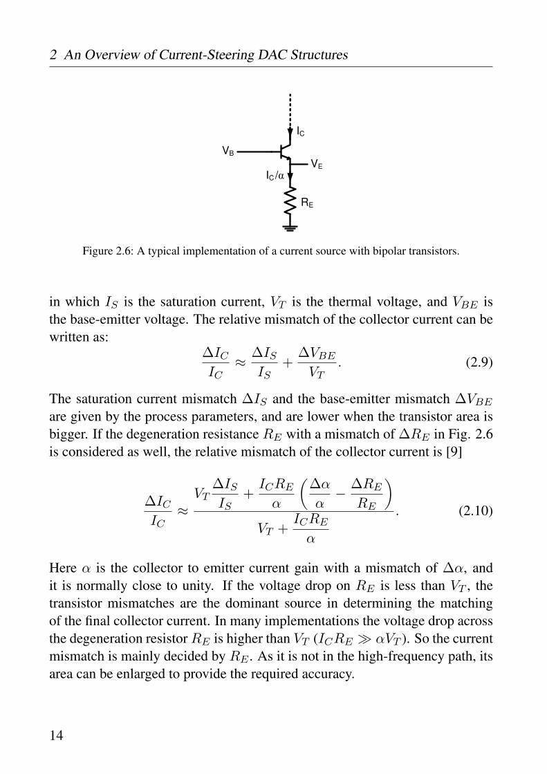
2 An Overview of Current-Steering DAC Structures
RE
VB
VE
IC
IC /α
Figure 2.6: A typical implementation of a current source with bipolar transistors.
in which IS is the saturation current, VT is the thermal voltage, and VBE isthe base-emitter voltage. The relative mismatch of the collector current can bewritten as:
∆IC
IC≈ ∆IS
IS+ ∆VBE
VT. (2.9)
The saturation current mismatch ∆IS and the base-emitter mismatch ∆VBE
are given by the process parameters, and are lower when the transistor area isbigger. If the degeneration resistance RE with a mismatch of ∆RE in Fig. 2.6is considered as well, the relative mismatch of the collector current is [9]
∆IC
IC≈
VT∆IS
IS+ ICRE
α
(∆α
α− ∆RE
RE
)
VT + ICRE
α
. (2.10)
Here α is the collector to emitter current gain with a mismatch of ∆α, andit is normally close to unity. If the voltage drop on RE is less than VT , thetransistor mismatches are the dominant source in determining the matchingof the final collector current. In many implementations the voltage drop acrossthe degeneration resistor RE is higher than VT (ICRE ≫ αVT ). So the currentmismatch is mainly decided by RE . As it is not in the high-frequency path, itsarea can be enlarged to provide the required accuracy.
14
2.4 Conclusion
2.3.2 Dynamic Error Sources
Dynamic output impedance and timing mismatches are actually the other sourcesof error at the DAC output. In a current-steering DAC implementation, it ispossible to formulate the deterioration based on the cell-dependent delay dif-ferences [11] and output-dependent delay differences [12]. Due to the complexnature of the problem and the sources generating such an error, abundant priorworks presented mathematical models to address this issue, e.g. [13], [14]. Thenext chapter explains this topic and provides a background helping the designof current source cells.
2.4 Conclusion
In this chapter, the most used architectures in current-steering DAC designsare briefly introduced. Based on simplicity, the binary method is rated thefirst, while segmented and unary structures are coming afterwards. When thebetter accuracy is required the rating is inversed and the unary realization issuperior, where segmented and then binary architectures are considered next toit. Because of complex implementation of a fully unary DAC, the segmentedstructure is mostly used at high-speed designs. However due to its simplicity,the focus of this work is more on a binary design. The main static error sourcesin a current source cell are studied as well. It was shown that usage of resistorsand transistors with larger area provides lower relative mismatch values in agiven process. The mismatches of a resistor and a bipolar current source areformulated as well.
15

16

![^]K[Ip^Q¸p^I¸vKSoKkK¸ ^P`k]>oS`^K^¸{p ... · ^]K[Ip^Q¸p^I¸vKSoKkK¸ ^P`k]>oS`^K^¸{p]¸ IKo>S[[SKkoK^¸*k`Qk>]]¸KkR>[oK^¸.SK¸u`^ * ¸ k ¸k]S^¸ >[K^Z> FoKS[p^Q¸^AloRKlSK¸p^I¸](https://static.unterlagen.site/doc/80x56/5e19005b0db62a47453c2ab8/kipqpivksokkk-pkoskp-kipqpivksokkk-pkoskp.jpg)


![KD d / K >/D/d KE^K>/ d &/E E / > ^d d D Ed^ &KZ d, z Z E ... › CLIENT_CL_Corp_3513EFE5_AF37_1D84_E3… · KD d / K >/D/d ^dZ d '/ Z WKZd î d Z ] } v Z ] ^ P ] } ( } } u ] } >](https://static.unterlagen.site/doc/80x56/60ba3e73c531c90c56690c14/kd-d-k-dd-kek-d-e-e-d-d-d-ed-kz-d-z-z-e-a.jpg)


