Defect Study of Hydrogen Ion Defect Study of Hydrogen Ion-Cutting of GaN Cutting of GaN O Moutanabbir 3 R Krause Rehberg 1 O. Moutanabbir 3 , R. Krause-Rehberg 1 , M. Jungmann 1, F.Süßkraut 1 , A. Guittoum 1 , M. Butterling 1 , W . Egger 2 , P. Sperr 2 , G. Kögel 2 1 Martin-Luther-University Halle-Wittenberg / Germany 2 Universität der Bundeswehr, Munich / Germany Universität der Bundeswehr, Munich / Germany 3 Max Planck Institute of Microstructure Physics, Halle / Germany R Martin-Luther-Universität Halle
Transcript
Defect Study of Hydrogen IonDefect Study of Hydrogen Ion--Cutting of GaNCutting of GaN
O Moutanabbir3 R Krause Rehberg1O. Moutanabbir3, R. Krause-Rehberg1, M. Jungmann1, F.Süßkraut1, A. Guittoum1, M. Butterling1,
2Universität der Bundeswehr, Munich / GermanyUniversität der Bundeswehr, Munich / Germany
3Max Planck Institute of Microstructure Physics, Halle / Germany
RKR
Martin-Luther-Universität Halle
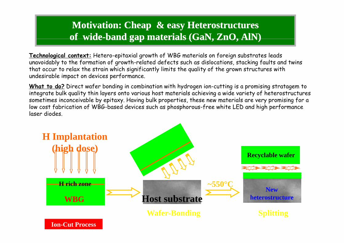
Motivation: Cheap & easy Heterostructures Motivation: Cheap & easy Heterostructures of wideof wide--band gap materials (GaN,band gap materials (GaN, ZnOZnO,, AlNAlN))
Technological context: Hetero-epitaxial growth of WBG materials on foreign substrates leads unavoidably to the formation of growth-related defects such as dislocations, stacking faults and twins
of wideof wide band gap materials (GaN, band gap materials (GaN, ZnOZnO, , AlNAlN))
that occur to relax the strain which significantly limits the quality of the grown structures with undesirable impact on devices performance.
What to do? Direct wafer bonding in combination with hydrogen ion-cutting is a promising stratagem to integrate bulk quality thin layers onto various host materials achieving a wide variety of heterostructures integrate bulk quality thin layers onto various host materials achieving a wide variety of heterostructures sometimes inconceivable by epitaxy. Having bulk properties, these new materials are very promising for a low cost fabrication of WBG-based devices such as phosphorous-free white LED and high performance laser diodes.
H Implantation (high dose)(high dose)
R
Recyclable wafer
WBG
H rich zone
Host substrateNew
heterostructure
~550°CRpRp
Wafer-Bonding SplittingIon-Cut Process
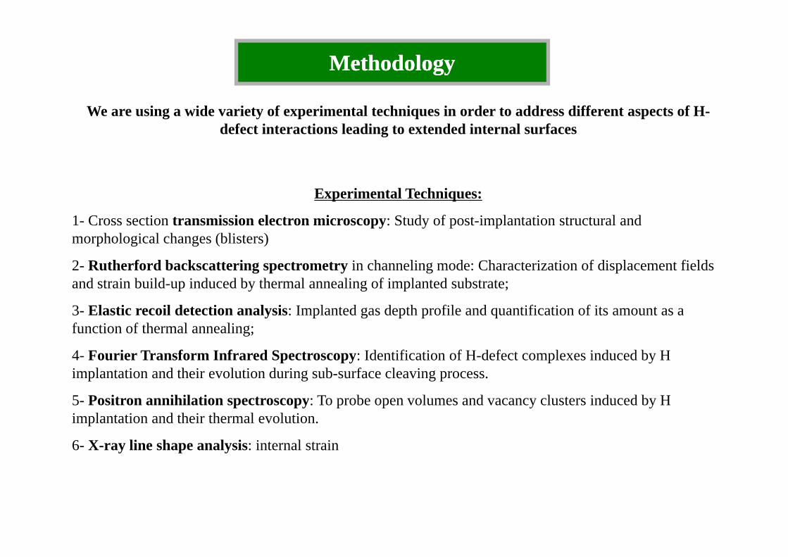
MethodologyMethodology
We are using a wide variety of experimental techniques in order to address different aspects of H-defect interactions leading to extended internal surfaces
Experimental Techniques:
1 C i i i i S d f i l i l d1- Cross section transmission electron microscopy: Study of post-implantation structural and morphological changes (blisters)
2- Rutherford backscattering spectrometry in channeling mode: Characterization of displacement fields d i b ild i d d b h l li f i l d band strain build-up induced by thermal annealing of implanted substrate;
3- Elastic recoil detection analysis: Implanted gas depth profile and quantification of its amount as a function of thermal annealing;
4- Fourier Transform Infrared Spectroscopy: Identification of H-defect complexes induced by H implantation and their evolution during sub-surface cleaving process.
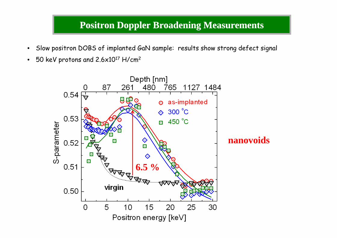
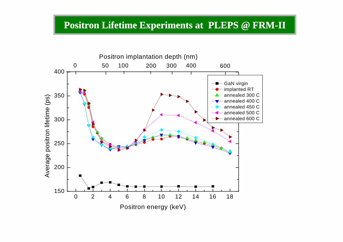
5- Positron annihilation spectroscopy: To probe open volumes and vacancy clusters induced by H5 Positron annihilation spectroscopy: To probe open volumes and vacancy clusters induced by H implantation and their thermal evolution.
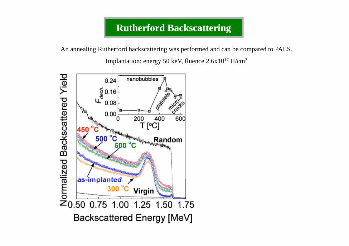
An annealing Rutherford backscattering was performed and can be compared to PALS.
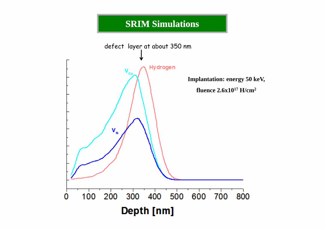
Implantation: energy 50 keV, fluence 2.6x10¹⁷ H/cm2
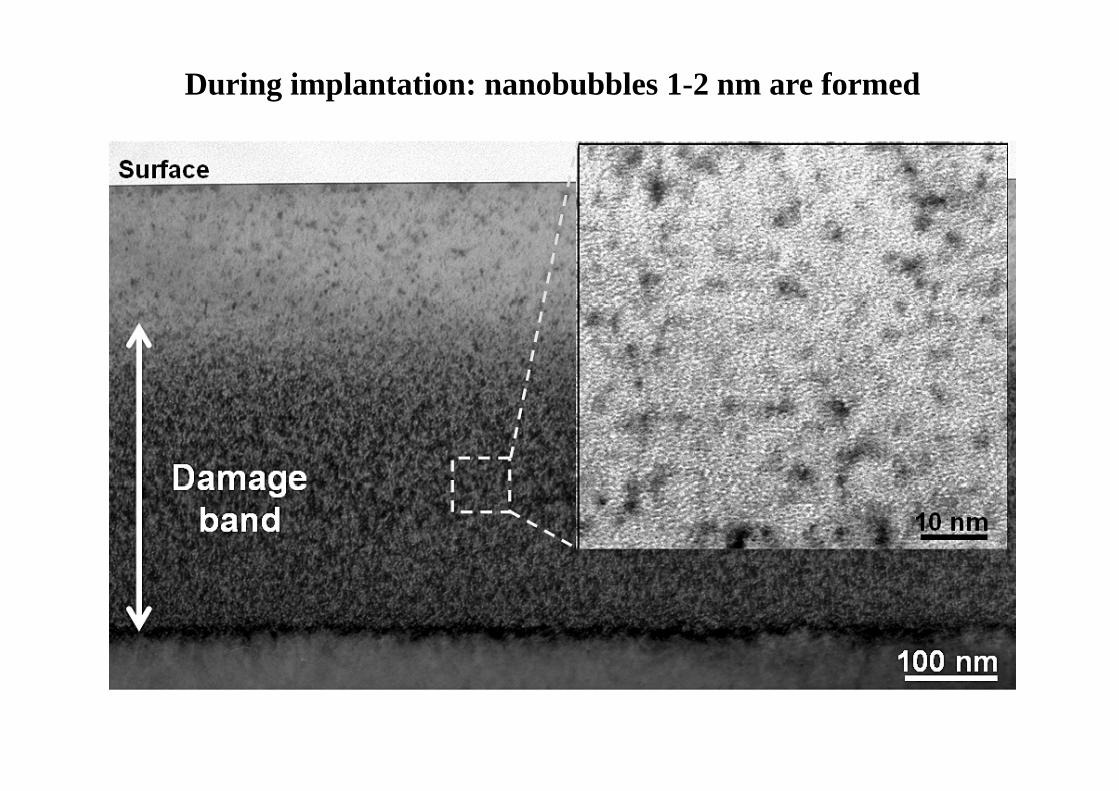
During implantation: nanobubbles 1-2 nm are formed
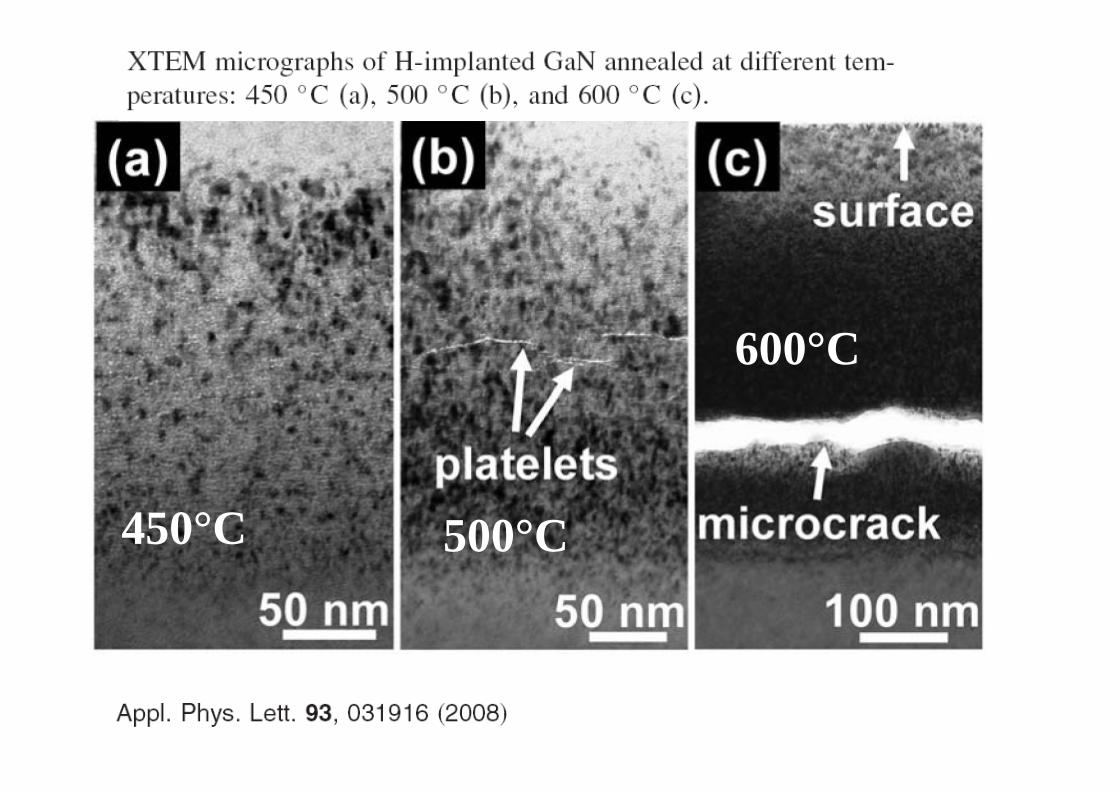
600°C
450°C 500°C
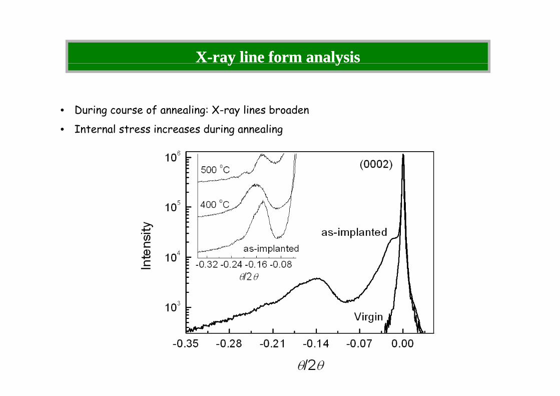
XX--ray line form analysisray line form analysisy yy y
Durin course of annealin : X ray lines broaden• During course of annealing: X-ray lines broaden
• Internal stress increases during annealing
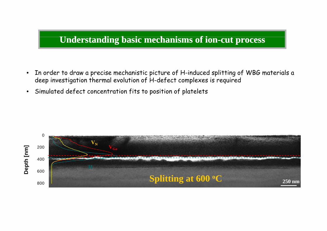
U d t di b i h i f iU d t di b i h i f i ttUnderstanding basic mechanisms of ionUnderstanding basic mechanisms of ion--cut processcut process
• In order to draw a precise mechanistic picture of H-induced splitting of WBG materials a deep investigation thermal evolution of H-defect complexes is required
Si l t d d f t t ti fit t iti f l t l t
High magnification XTEM image showing id ( b bbl ) hi h
• Simulated defect concentration fits to position of platelets
s) annealed 300 C annealed 400 C annealed 450 C annealed 500 Cannealed 600 C
250
300
ositr
on li
fe
200
Aver
age
p
0 2 4 6 8 10 12 14 16 18150
A
Positron energy (keV)
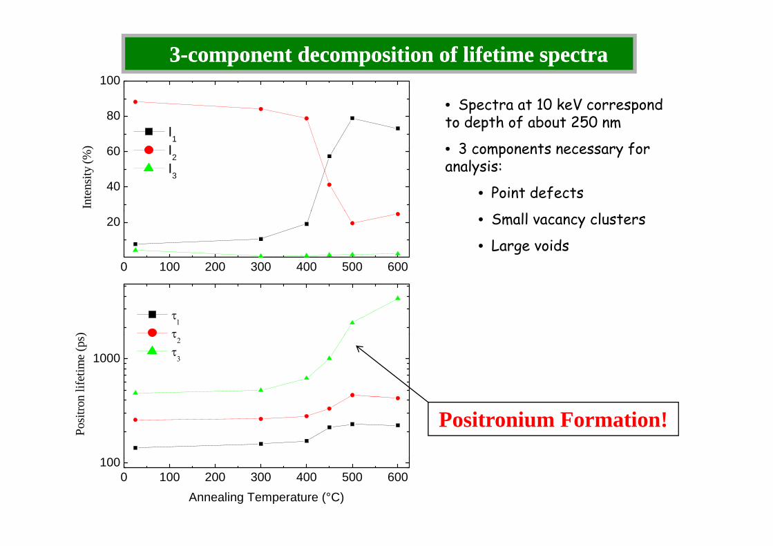
33--component decomposition of lifetime spectracomponent decomposition of lifetime spectra100
60
80 I1I)
• Spectra at 10 keV correspond to depth of about 250 nm
• 3 components necessary for
40
60 I2 I3
Inte
nsity
(%) • 3 components necessary for
analysis:
• Point defects
0 100 200 300 400 500 600
20 • Small vacancy clusters
• Large voids
τ1
τ)
1000
τ2
τ3
n lif
etim
e (p
s)
Positronium Formation!
100
Posi
tron
0 100 200 300 400 500 600100
Annealing Temperature (°C)
C l iC l iConclusionsConclusions
t t l t d f i litti f G N b H i l t ti
High magnification XTEM image showing id ( b bbl ) hi h
• structural study of ion splitting of GaN by H implantation
• vacancy clustering during the implantation: 1–2 nm nanobubbles
• further clustering during annealing nanovoids (or nanobubbles) which appear bright.
• further clustering during annealing
• 300–450 °C: strong enhancement of strain-induced lattice distortion
• formation of platelets: partial relief of the strain • formation of platelets: partial relief of the strain
• extended internal surfaces develop around 550 °C
• leading to splitting of 340-nm-thick GaN layer leading to splitting of 340 nm thick GaN layer
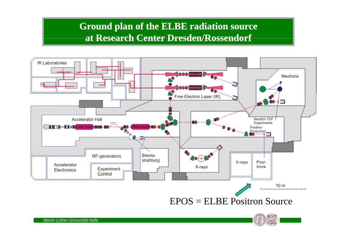
Ground plan of the ELBE Ground plan of the ELBE radiation source radiation source at Research Center Dresden/Rossendorfat Research Center Dresden/Rossendorfat Research Center Dresden/Rossendorfat Research Center Dresden/Rossendorf
EPOS = ELBE Positron Source
Martin-Luther-Universität Halle
EPOS ELBE Positron Source
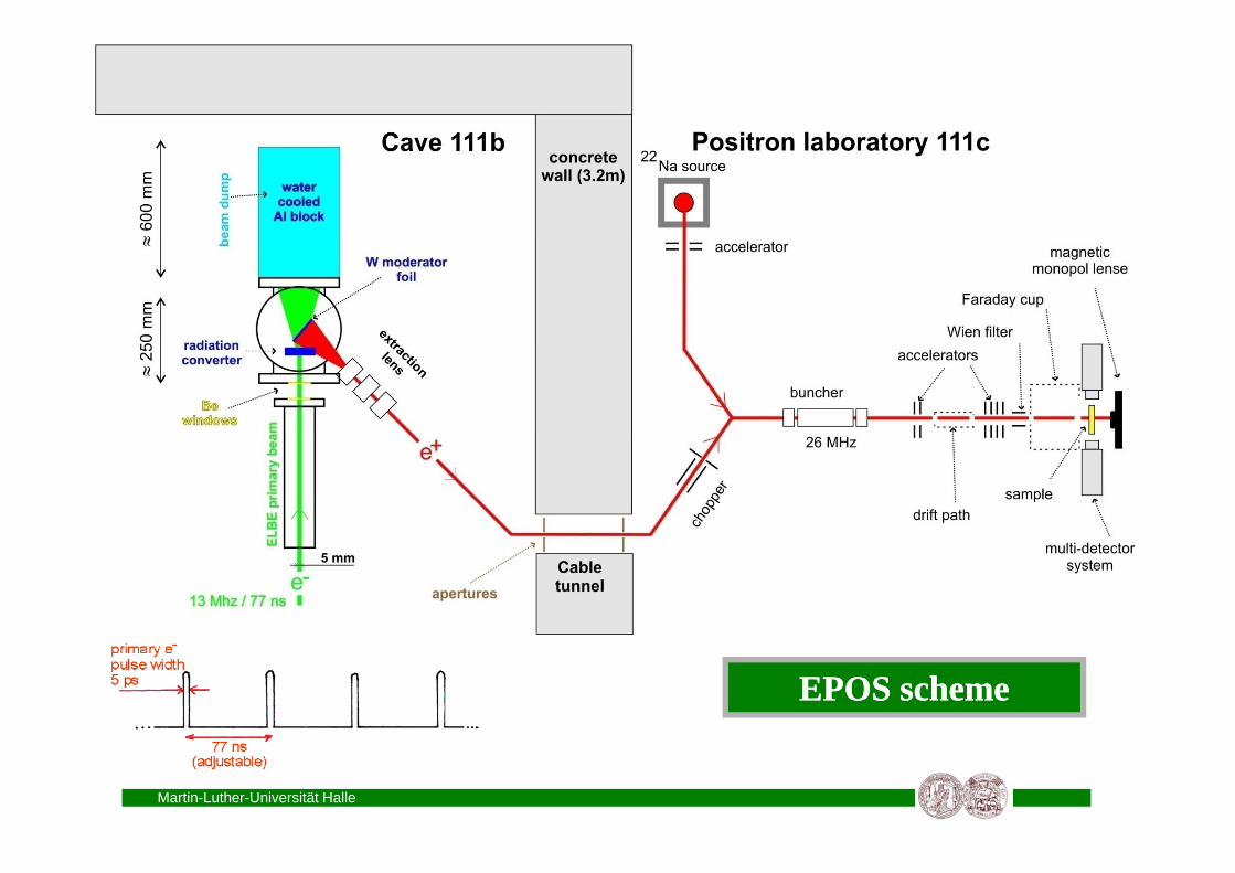
EPOS scheme EPOS scheme
Martin-Luther-Universität Halle
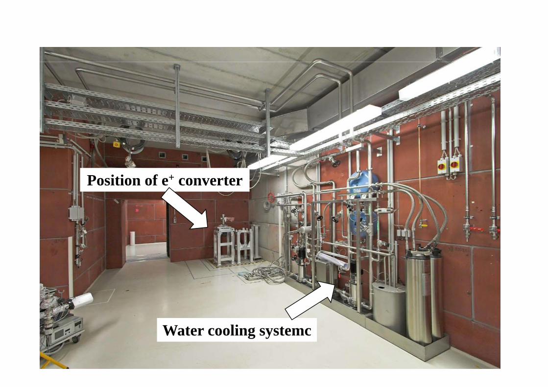
Cave 111b
Position of e+ converter
W liWater cooling systemc
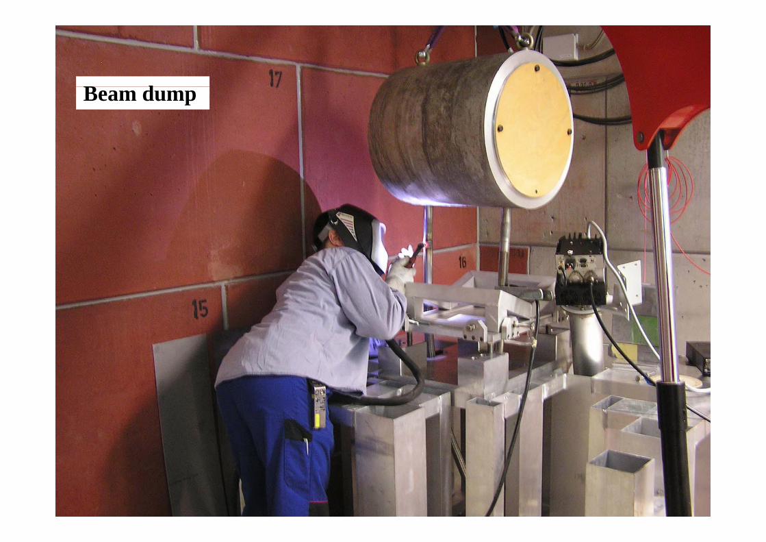
B dBeam dump
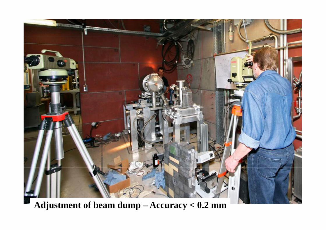
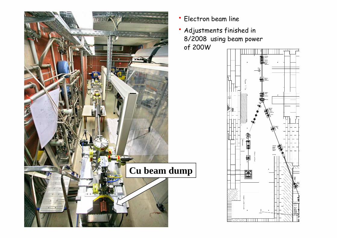
Adjustment of beam dump – Accuracy < 0.2 mm
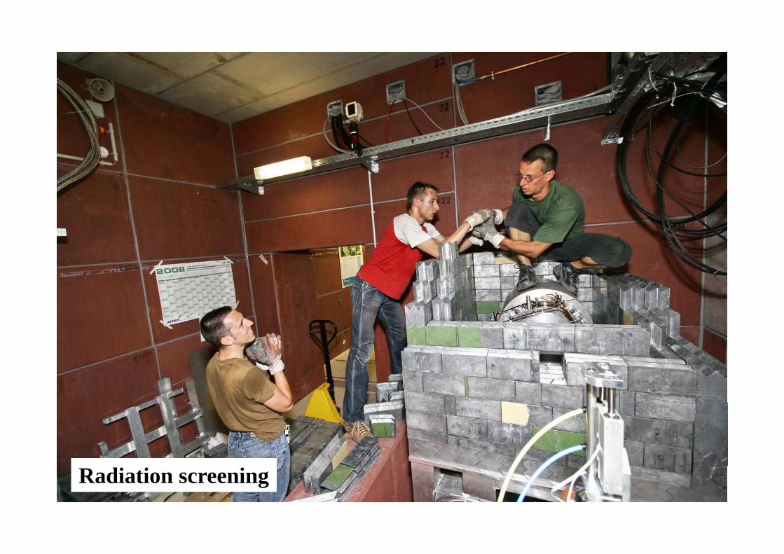
Radiation screening
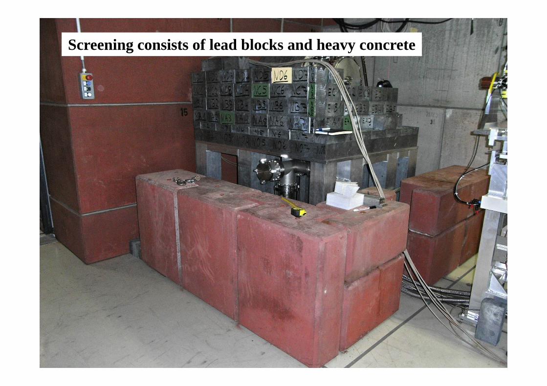
Screening consists of lead blocks and heavy concrete
• Electron beam line
• Adjustments finished in 8/2008 using beam power 8/2008 using beam power of 200W
Cu beam dumpCu beam dump
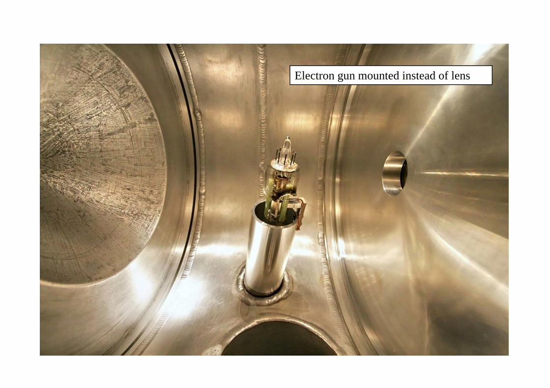
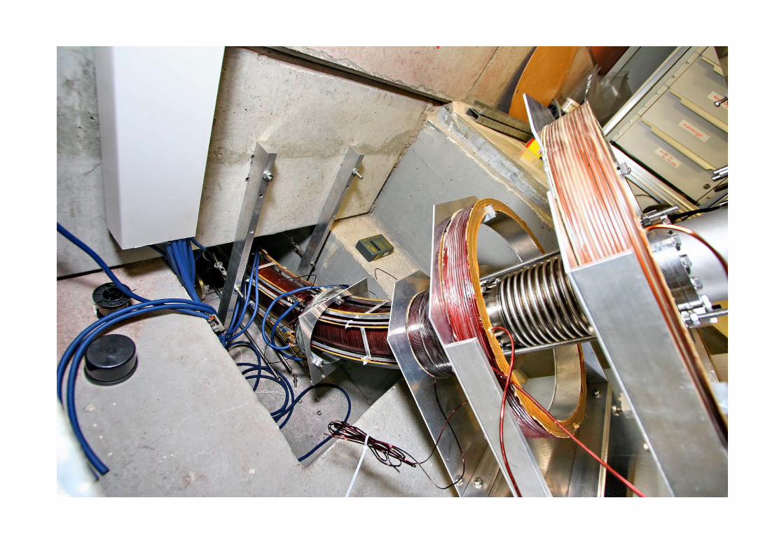
Electron gun mounted instead of lens
Future PlansFuture Plans
• Electron gun until the end of the vacuum tube
• 22-Na beam source with moderator should be built in instead of electron-positron converter (save ELBE beam time)
• ELBE-beam time in December (14 -19 12 ): Generating positrons by ELBE electron ELBE beam time in December (14. 19.12.): Generating positrons by ELBE electron beam in low-power mode (diagnostic mode)
• Measure energy and time spread of positron bunches
h l h • Finish sample chamber design
• Further improvement of digital lifetime and Doppler measurement
• Test scintillators (LSO ZnO )Test scintillators (LSO, ZnO, ...)