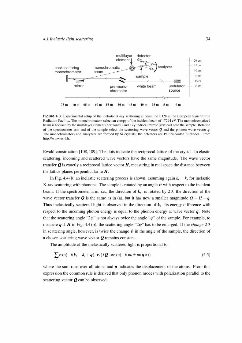
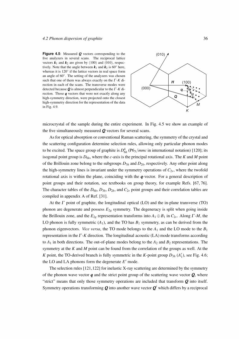
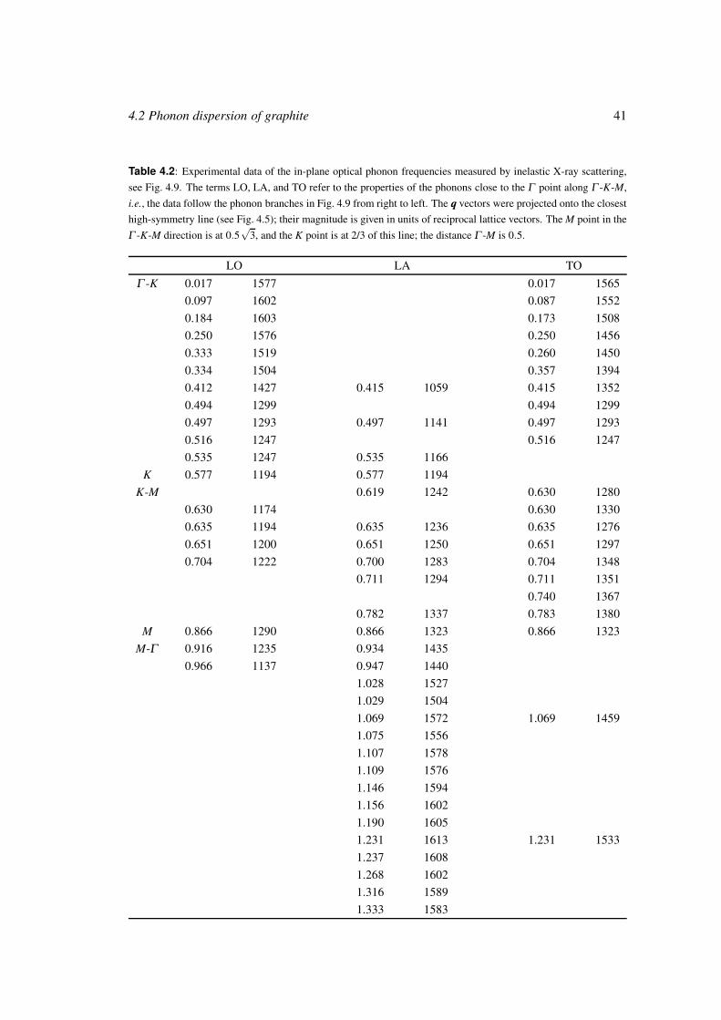
Vibrational properties of carbon nanotubes and graphite vorgelegt von Diplom-Physikerin Janina Maultzsch aus Berlin von der Fakult¨ at II − Mathematik und Naturwissenschaften der Technischen Universit¨ at Berlin zur Erlangung des akademischen Grades Doktor der Naturwissenschaften − Dr. rer. nat. − genehmigte Dissertation Promotionsausschuss: Vorsitzender: Prof. Dr. Siegfried Hess Berichter: Prof. Dr. Christian Thomsen Berichter: Prof. Dr. Wolfgang Richter Tag der wissenschaftlichen Aussprache: 15. Juni 2004 Berlin 2004 D83
Transcript
Vibrational properties of carbon nanotubes
and graphite
vorgelegt von
Diplom-Physikerin
Janina Maultzsch
aus Berlin
von der Fakultat II −Mathematik und Naturwissenschaften
der Technischen Universitat Berlin
zur Erlangung des akademischen Grades
Doktor der Naturwissenschaften
− Dr. rer. nat. −
genehmigte Dissertation
Promotionsausschuss:
Vorsitzender: Prof. Dr. Siegfried Hess
Berichter: Prof. Dr. Christian Thomsen
Berichter: Prof. Dr. Wolfgang Richter
Tag der wissenschaftlichen Aussprache: 15. Juni 2004
Berlin 2004
D83
ii
Zusammenfassung
In dieser Arbeit werden die Phononen von Kohlenstoff-Nanotubes und Graphit untersucht.
Kohlenstoff-Nanotubes sind quasi-eindimensionale Kristalle und bestehen aus einer oder meh-
reren Graphit-Ebenen, die zu einem Zylinder aufgerollt sind. Deshalb konnen in erster
Naherung viele Eigenschaften der Nanotubes von Graphit hergeleitet werden, indem das Nano-
tube als ein schmales Rechteck aus Graphit mit periodischen Randbedingungen betrachtet wird.
Die hier verwendeten experimentellen Methoden sind Raman-Spektroskopie und fur
Graphit inelastische Rontgenstreuung. Das Ramanspektrum von Kohlenstoff-Nanotubes wurde
bisher nicht im Detail verstanden, insbesondere kann es nicht in herkommlicher Weise mit der
Streuung von Γ -Punkt Phononen widerspruchsfrei erklart werden. Abgesehen von der soge-
nannten Atmungsmode, einer niederenergetischen, radialen Schwingung des gesamten Tubes,
sind die Ramanpeaks keine einfachen Lorentz-formigen Moden, sondern komplexe, relativ
breite Peaks. Andererseits gibt es nur zwei Phononen, die in diesem hochenergetischen Bereich
des Spektrums aus Symmetrie-Grunden erlaubt sind. Eine weitere ungewohnliche Eigenschaft
ist die starke Abhangigkeit des Ramanspektrums von der Energie des anregenden Lasers. Dies
betrifft nicht nur die Intensitat des Spektrums, wie in gewohnlicher resonanter Ramanstreuung,
sondern auch die Frequenz der Ramanmoden und ihre Linienform. Ebenso sind bei gleicher
Anregungsenergie die Spektren in Stokes- und Anti-Stokes-Streuung unterschiedlich.
Diese Eigenschaften des Ramanspektrums werden in dieser Arbeit mit Hilfe von Defekt-
induzierter, doppelresonanter Ramanstreuung erklart. Dabei fuhrt die elastische Streuung
an einem Defekt dazu, dass nicht nur Phononen vom Γ -Punkt zum Spektrum erster Ord-
nung beitragen konnen, sondern Phononen aus der gesamten Brillouin-Zone. Fur diejenigen
Phononen, die zu einer Doppelresonanz fuhren, ist die Streuwahrscheinlichkeit am starksten
und ergibt daher einen Peak im Spektrum. Wenn die Anregungsenergie geandert wird, andert
sich auch die Bedingung fur die Doppelresonanz, entsprechend der elektronischen Bandstruk-
tur und der Phononendispersion. Dadurch werden andere Phononen bevorzugt, und die Ra-
manpeaks verschieben sich. Im Prinzip ist es damit moglich, die Phononendispersion oder
einen Teil davon durch Variation der Laserwellenlange zu messen. Das Doppelresonanz-
Modell erklart auch alle weiteren Eigenschaften des Ramanspektrums ohne zusatzliche An-
Zusammenfassung iv
nahmen: Selbst im Falle von nur einem Phononenzweig werden Mehrfach-Peaks vorherge-
sagt, die gleichzeitig durch mehrere, leicht unterschiedliche Doppelresonanz-Bedingungen her-
vorgerufen werden.
Neben der elektronischen Bandstruktur ist die Phononendispersion selbst bestimmend fur
die Doppelresonanz. Uberraschenderweise gab es bisher selbst fur Graphit keine vollstandigen
experimentellen Daten in der Literatur, unter anderem, weil nur etwa 100 µm große Einkristalle
von Graphit existieren. Entsprechend widerspruchlich sind die theoretischen Vorhersagen. Wir
waren in der Lage, diese Widerspruche zu losen, indem wir die optischen Phononen mit in-
elastischer Rontgenstreuung in der gesamten Brillouin-Zone gemessen haben.
Wir kombinieren nun die Kenntnisse uber die Symmetrie-Eigenschaften (Auswahlregeln),
die elektronische Bandstruktur und die Phononendispersionen, um die Ramanspektren mit dem
Doppelresonanz-Modell explizit zu berechnen. Dabei finden wir eine sehr gute Ubereinstim-
mung mit dem Experiment. In fruheren Interpretationen der Ramanspektren wurde die starke
Abhangigkeit von der Laserenergie mit der selektiven Anregung von unterschiedlichen Nan-
otubes erklart, da zu dieser Zeit die meisten Experimente an Proben mit vielen verschiede-
nen, zu Bundeln zusammengeschlossenen Tubes durchgefuhrt wurden. In dieser Interpretation
wurden die Spektren eines einzelnen Nanotubes nicht von der Anregungsenergie abhangen.
Hier zeigen wir jedoch durch systematische Messungen an einem einzelnen Tube, dass das Ra-
manspektrum dieses Tubes ebenfalls variiert. Die besonderen Eigenschaften des Ramanspek-
trums, vor allem die Abhangigkeit von der Laserenergie, sind also ein Effekt eines einzelnen
Nanotubes, wie von der Doppelresonanz vorhergesagt.
List of publications
Carbon Nanotubes: Basic Concepts and Physical Properties
S. Reich and C. Thomsen and J. Maultzsch,
Wiley-VCH, Berlin (2004).
Phonon dispersion in graphite
J. Maultzsch, S. Reich, C. Thomsen, H. Requardt, and P. Ordejon,
Phys. Rev. Lett. 92, 075501 (2004).
High-energy phonon branches of an individual metallic carbon nanotube
J. Maultzsch, S. Reich, U. Schlecht, and C. Thomsen,
Phys. Rev. Lett. 91, 087402 (2003).
The radial breathing mode frequency in double-walled carbon nanotubes: an analytical
approximation
E. Dobardzic, J. Maultzsch, I. Milosevic, C. Thomsen, and M. Damnjanovic,
phys. stat. sol., 237, R7 (2003).
Quantum numbers and band topology of nanotubes
M. Damnjanovic, I. Milosevic, T. Vukovic, and J. Maultzsch,
J. Phys. A: Math. Gen. 36, 5707 (2003).
Raman characterization of boron-doped multiwalled carbon nanotubes
J. Maultzsch, S. Reich, C. Thomsen, S. Webster, R. Czerw, D. L. Carroll, S. M. C. Vieira,
P. R. Birkett, and C. A. Rego,
Appl. Phys. Lett 81, 2647 (2002).
Tight-binding description of graphene
S. Reich, J. Maultzsch, C. Thomsen, and P. Ordejon,
Phys. Rev. B 66, 035412 (2002).
List of publications vi
Raman scattering in carbon nanotubes revisited
J. Maultzsch, S. Reich, and C. Thomsen,
Phys. Rev. B 65, 233402 (2002).
Phonon dispersion of carbon nanotubes
J. Maultzsch, S. Reich, C. Thomsen, E. Dobardzic, I. Milosevic, and M. Damnjanovic,
Solid State Comm. 121, 471 (2002).
Chirality-selective Raman scattering of the D mode in carbon nanotubes
J. Maultzsch, S. Reich, and C. Thomsen,
Phys. Rev. B 64, 121407(R) (2001).
Resonant Raman scattering in GaAs induced by an embedded InAs monolayer
J. Maultzsch, S. Reich, A. R. Goni, and C. Thomsen,
Phys. Rev. B 63, 033306 (2001).
Manuscripts under review
Chirality distribution and transition energies of carbon nanotubes
H. Telg, J. Maultzsch, S. Reich, F. Hennrich, and C. Thomsen,
submitted to Phys. Rev. Lett. (2004).
Double-resonant Raman scattering in graphite: interference effects, selection rules and
phonon dispersion
J. Maultzsch, S. Reich, and C. Thomsen,
submitted to Phys. Rev. B (2004).
Resonant Raman spectroscopy of nanotubes
C. Thomsen, S. Reich, and J. Maultzsch,
submitted to Philosophical Transactions of the Royal Society (2004).
The strength of the radial breathing mode in single-walled carbon nanotubes
M. Machon, S. Reich, J. Maultzsch, P. Ordejon, and C. Thomsen,
submitted to Phys. Rev. Lett. (2003).
List of publications vii
Conference proceedings
Vibrational properties of double-walled carbon nanotubes
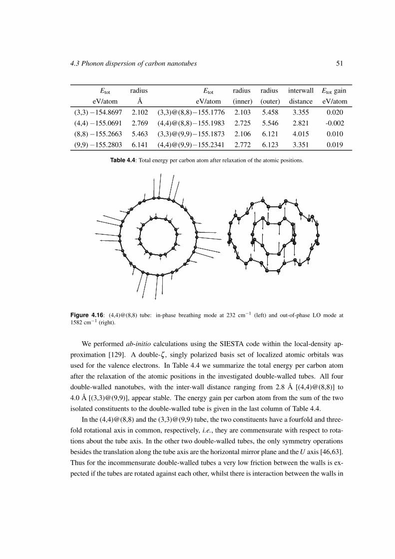
J. Maultzsch, S. Reich, P. Ordejon, R. R. Bacsa, W. Bacsa, E. Dobardzic, M. Damn-
janovic, and C. Thomsen,
Proc. of the XVIIth Intern. Winterschool on Electronic Properties of Novel Materials,
Kirchberg, Austria, ed. by H. Kuzmany, J. Fink, M. Mehring, and S. Roth, (AIP 685),
324 (2003).
Double-resonant Raman scattering in an individual carbon nanotube
C. Thomsen, J. Maultzsch, and S. Reich,
ibid., p. 225.
Raman measurements on electrochemically doped single-wall carbon nanotubes
P.M. Rafailov, M. Stoll, J. Maultzsch, and C. Thomsen,
ibid., p. 135.
Hexagonal diamond from single-walled carbon nanotubes
S. Reich, P. Ordejon, R. Wirth, J. Maultzsch, B. Wunder, H.-J. Muller, C. Lathe, F.
Schilling, U. Detlaff-Weglikowska, S. Roth, and C. Thomsen,
ibid., p. 164.
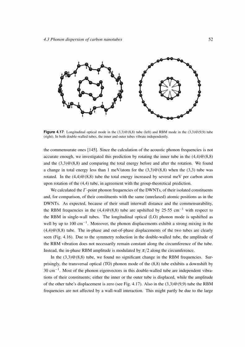
Raman characterization of nitrogen-doped multiwalled carbon nanotubes
S. Webster, J. Maultzsch, C. Thomsen, J. Liu, R. Czerw, M. Terrones, F. Adar, C. John,
A. Whitley, and D. L. Carroll,
Mat. Res. Soc. Symp. Proc. 772, M7.8.1 (2003).
Double-resonant Raman scattering in single-wall carbon nanotubes
J. Maultzsch and S. Reich and C. Thomsen,
Proc. 26th ICPS, ed. by A. R. Long and J. H. Davies, (Institute of Physics Publishing,
Bristol, UK), D209 (2002).
Optical properties of 4 A-diameter single-wall nanotubes
M. Machon, S. Reich, J. Maultzsch, P. M. Rafailov, C. Thomsen, D. Sanchez-Portal, and
P. Ordejon,
Proc. of the XVIth Intern. Winterschool on Electronic Properties of Novel Materials,
Kirchberg, Austria, ed. by H. Kuzmany, J. Fink, M. Mehring, and S. Roth, (AIP 633),
275 (2002).
Pressure and polarization-angle dependent Raman spectra of aligned single-wall carbon
nanotubes in AlPO4-5 crystal channels
List of publications viii
P. M. Rafailov, J. Maultzsch, M. Machon, S. Reich, C. Thomsen, Z. K. Tang, Z. M. Li,
and I. L. Li,
ibid., p. 290.
Origin of the high-energy Raman modes in single-wall carbon nanotubes
J. Maultzsch, C. Thomsen, S. Reich, and M. Machon,
ibid., p. 352.
The dependence on excitation energy of the D-mode in graphite and carbon nanotubes
C. Thomsen, S. Reich, and J. Maultzsch,
Proc. of the XVth Intern. Winterschool on Electronic Properties of Novel Materials,
Kirchberg, Austria, ed. by H. Kuzmany, J. Fink, M. Mehring, and S. Roth, (AIP 591),
376 (2001).
Resonant Raman scattering in an InAs/GaAs monolayer structure
J. Maultzsch, S. Reich, A. R. Goni, and C. Thomsen,
Proc. 25th ICPS, ed. by N. Miura and T. Ando (Springer Berlin), 697 (2001).
Carbon appears in several crystalline modifications, as a result of its flexible electron configu-
ration. The carbon atom has six electrons; the 2s orbital and two or three of the 2p orbitals can
form an sp2 or sp3 hybrid, respectively. The sp3 configuration gives rise to the tetrahedrally
bonded structure of diamond. The sp2 orbitals lead to strong in-plane bonds of the hexagonal
structure of graphite and the remaining p-like orbital to weak bonds between the planes. Be-
sides diamond and graphite, other modifications of crystalline carbon have been found, among
them the so-called buckyballs [1] and, first reported in 1991 by Iijima [2], carbon nanotubes.
Soon after their discovery in multiwall form, carbon nanotubes consisting of one single layer
were found [3,4]. The most famous one of the buckyballs is probably C60, a spherical molecule
formed by pentagons and hexagons, out of which single C60 crystals have been produced [5].
Carbon nanotubes are quasi-one dimensional crystals with the shape of hollow cylinders
made of one or more graphite sheets; they are typically µm in length and 1 nm in diameter.
Along the cylinder axis, they can therefore be regarded as infinitely long (approximately 104
atoms along 1 µm), whereas along the circumference there are only very few atoms (≈ 20).
This gives rise to discrete wave vectors in the circumferential direction and quasi-continuous
wave vectors along the tube axis. Although carbon nanotubes consist of merely carbon atoms,
their physical properties can vary significantly, depending sensitively on the microscopic struc-
ture of the tube. Most prominent is their metallic or semiconducting character: roughly speak-
ing 2/3 of the possible nanotube structures are semiconducting and 1/3 are metallic. Carbon
nanotubes exhibit remarkable physical properties. They were reported to carry electric cur-
rents up to 109 A/cm2 [6, 7]. Furthermore, nanotube ropes are of extraordinary mechanical
strength with an elastic modulus on the order of 1 TPa, and a shear modulus of approximately
1 GPa [8,9]. Therefore, they are extremely stiff along their axis but easy to bend perpendicular
to the axis. The shear modulus in the ropes can be enlarged by introducing bonds between the
tubes by electron beam irratiation [10].
The many possible applications of carbon nanotubes both on the nanometer scale and in
the macroscopic range attract great attention. Some of them have been realized on an industry
scale already, whereas others still require sophisticated preparation. The latter include single-
1 Introduction 4
nanotube electronic devices such as field-effect transistors [11] or even logic circuits [12]. In
so-called actuators, an electrolytically doped nanotube paper is bent by an applied bias [13,14].
Furthermore, carbon nanotubes were suggested to be used as torsional springs [15,16] or as sin-
gle vibrating strings for ultrasmall force sensing. A major difficulty for these applications is the
variety of nanotube structures that are produced simultaneously; in particular, a growth method
which determines whether the tubes will be metallic or semiconducting is still not available.
Instead, the production methods yield tube ensembles where presumably all nanotube struc-
tures are equally distributed, and the tubes are typically found in bundles. Other applications
like nanotube field emitters or reinforcing materials by adding carbon nanotubes, do not require
specific isolated tubes and are thus easier to realize.
Beyond the variety of applications, carbon nanotubes are interesting from a fundamental-
physics point of view. Their one-dimensional character has been manifested in many exper-
iments like scanning-tunneling spectroscopy, where the singularities in the density of states
typical for one dimension have been measured [17–19]. They appear an ideal system for the
study of Luttinger liquid behavior [20, 21]. Ballistic transport at room temperature up to sev-
eral µm was reported [22]. Alternatively, defects or electrical contacts can act as boundaries,
and zero-dimensional effects such as Coulomb blockade are observed [23, 24]. In contrast to
many quasi-one-dimensional systems in semiconductor physics, where carriers are artificially
restricted to a one-dimensional phase space by sophisticated fabrication like cleaved-edge over-
growth [25, 26] or experiments in the quantum-Hall regime [27], carbon nanotubes are natural
quasi-one-dimensional systems with ideal periodic boundary conditions along the circumfer-
ence. Furthermore, they have a highly symmetric microscopic structure which can be regarded
a realization of the so-called line groups that were introduced to describe the symmetry prop-
erties of mono-periodic crystals [28–30].
Since carbon nanotubes were first reported in 1991, research in this field has made tremen-
dous progress during the last years regarding both applications and fundamental properties [31].
This includes improved control over growth conditions (for a review see [32, 33]), the ability
to deposite nanotubes onto specific sites of a substrate, to debundle the tubes and measure
them individually [34], and, very recently, to prevent tubes from rebundling by enclosing them
into a surfactant [35]. The latter allowed key experiments in the optical characterization, the
observation of photoluminescence from the band gap of semiconducting tubes [36–39], and
investigations of the carrier dynamics by time-resolved optical spectroscopy [40, 41]. Further-
more, given a stable solution of isolated nanotubes, metallic tubes could be separated from
semiconducting ones by electrophoresis [42].
The third fundamental characteristics of a crystal, besides the transport and optical prop-
erties mentioned above, are the vibrational and elastic properties. For example, the long-
1 Introduction 5
wavelength acoustic phonons give the elastic moduli. Moreover, the phonon spectrum de-
termines the thermal properties and influences the non-radiative relaxation of excited carriers
and electronic transport. Raman scattering is a powerful tool study the vibrational properties
of a crystal and provides deep insight into the fundamental physical processes that take place.
The Raman process includes absorption and emission of light as well as inelastic scattering of
electrons by phonons (or other quasi-particles like magnons and plasmons). Thus information
on both electronic and vibrational properties and on electron-phonon interaction is obtained.
If the details of the Raman process are well understood, the experiments can also be used for
characterizing the sample.
Although one would expect a large number of phonon modes in the Raman spectrum of car-
bon nanotubes due to the confinement, there are in fact only three major bands in the first-order
spectrum. This is a consequence of the high symmetry of the nanotube, leading to selection
rules that prohibit most of the phonon modes in the Raman process. Because of the small mass
of the carbon atoms combined with strong carbon-carbon bonds, the phonon frequencies are
much larger than what is typically observed in semiconductors like GaAs or Si. The strongest
Raman modes are the radial breathing mode (a breathing-like vibration of the entire tube)
around 200 cm−1, and in the high-energy range the disorder-induced D mode (1350 cm−1) and
the high-energy modes (1600 cm−1). The Raman spectrum of carbon nanotubes has a num-
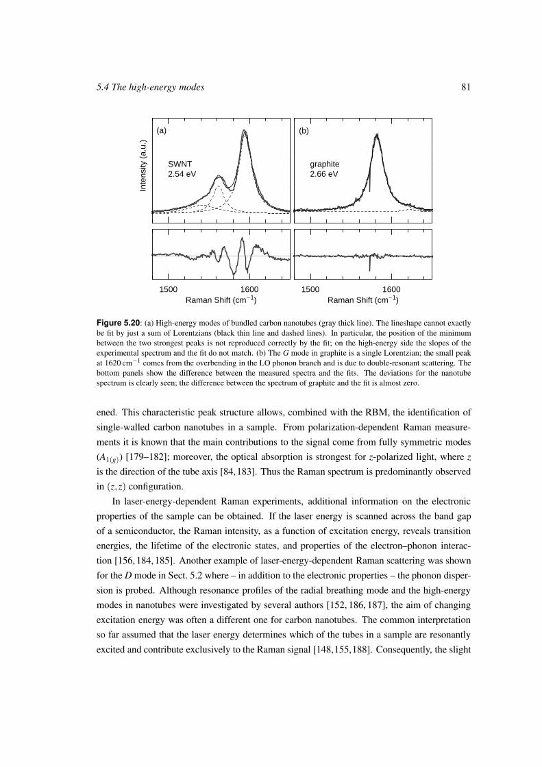
ber of peculiar properties. The first-order modes – except for the radial breathing mode – are
not composed by single Lorentzian peaks but have a rather complex line shape. In particular,
the high-energy mode consists of a multiple-peak structure that cannot simply be explained by
the two allowed first-order Raman modes. It changes dramatically with laser energy, which
was previously attributed to the selective excitation of metallic and semiconducting nanotubes.
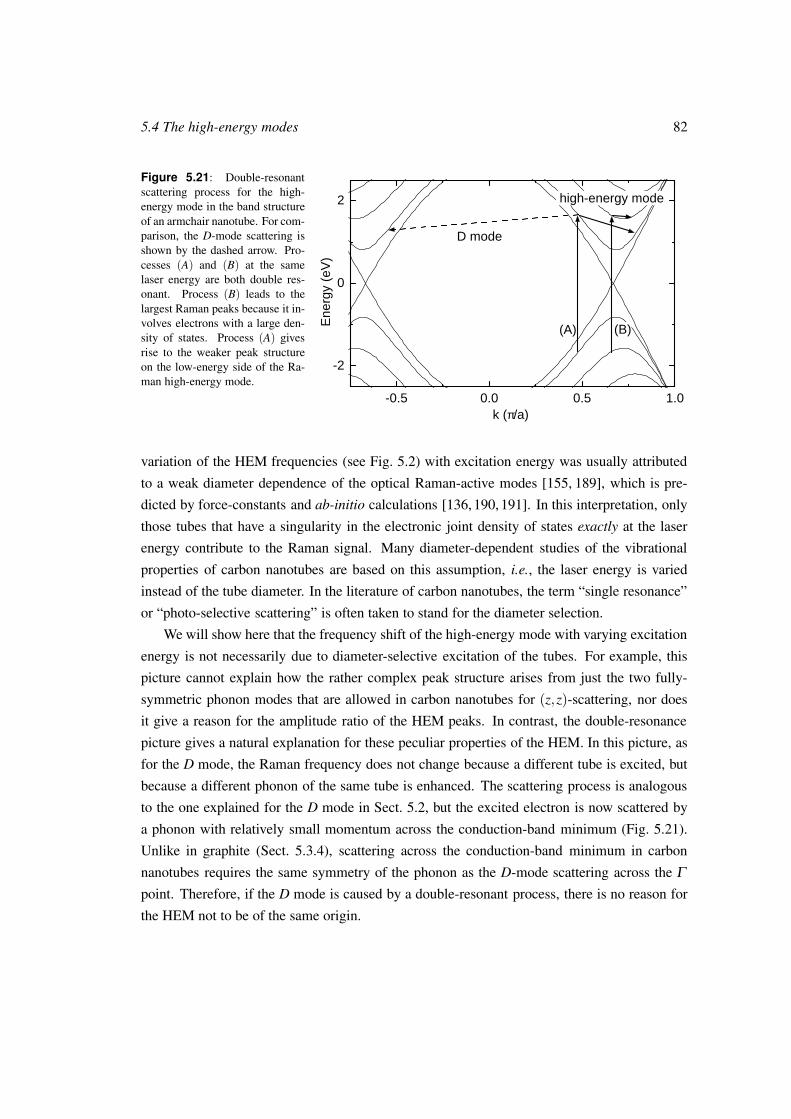
Even more surprising is the shift of the high-energy mode frequencies with excitation energy.
In spite of a large number of Raman studies in carbon nanotubes, the origin of the spectra
was not fully understood. In particular, it was not clear whether the characteristics of the na-
notube spectra, like the excitation-energy dependence, were results of averaging the properties
of many tubes measured simultaneously in tube ensembles or whether these effects would be
observed in single nanotubes as well. The proposal of defect-induced, double-resonant Raman
scattering as the origin of the entire first-order spectrum in carbon nanotubes at the beginning
of this thesis has led to controverse discussions [43–45]. This concept attributes the strong
laser-energy dependence of the Raman modes to single-tube effects rather than to a selective
excitation of different tubes. Besides the electronic band structure, the most important ingre-
dient to the double-resonant Raman process is the phonon dispersion. Surprisingly, it had not
even in graphite been determined experimentally, and theories were contradictory. Here we
1 Introduction 6
want to solve these questions and develop a consistent description of the Raman scattering
mechanism in carbon nanotubes.
To understand the Raman processes in carbon nanotubes, a profound knowledge of their
symmetry properties is needed. First, the selection rules for electron-photon and electron-
phonon interactions can be derived, which give rise to a systematic understanding of allowed
and forbidden processes, independent of a specific model or approximation. Second, the
symmetry-based treatment provides a simple and elegant way to describe quasi-particle states
in the nanotube and their interaction. We devote Chap. 2 to the symmetry properties of carbon
nanotubes [46], after a brief explanation of their geometrical structure and the construction of
the Brillouin zone. We discuss the line-group formalism and two different sets of quantum
numbers developed by Damnjanovic et al. [47], which both are used in this work depend-
ing on the particular problem. Since resonant Raman scattering depends on the details of
the electronic band structure, we will briefly review the electronic properties of carbon nan-
otubes in Chap. 3 as far as we will need them in the discussion of the scattering processes.
We investigate in Chap. 4 the phonons themselves, going back to graphite as the reference
material to carbon nanotubes. We measured for the first time the entire optical phonon disper-
sion in all high-symmetry directions in the graphite plane. These measurements had become
possible by the recently developed experimental technique of inelastic X-ray scattering. Our
experimental results solve long-standing discrepancies between different theoretical models.
We performed force-constants calculations of the nanotube phonon dispersion. Furthermore,
we briefly discuss ab-initio calculations of the phonon frequencies in double-walled carbon
nanotubes. Finally, we can combine the understanding obtained on symmetry, electronic and
vibrational properties of carbon nanotubes to work out the details of the Raman scattering pro-
cesses in Chap. 5. In particular, we will address the question of single and double-resonant
scattering and, closely related, the distinction between single-tube and tube-ensemble effects.
The double-resonance picture of the disorder-induced D mode is further developed, using the
experimental results of the graphite phonon dispersion to calculate the Raman spectra. For
the high-energy modes, the key experiments to distinguish between double and single-resonant
scattering are Raman measurements on the same individual tube at varying laser wavelengths.
The results give clear evidence for the double-resonant nature of the Raman modes, and we
show that by changing the excitation energy part of the phonon dispersion of a metallic tube
can be mapped. Finally, the absolute Raman cross section of the radial breathing mode is
measured and compared with ab-initio calculations.
2 Symmetry
Carbon nanotubes are hollow cylinders of graphite sheets. They can be viewed as single
molecules, regarding their small size (∼ nm in diameter and ∼ µm length), or as quasi-one di-
mensional crystals with translational periodicity along the tube axis. There are infinitely many
ways to roll a sheet into a cylinder, resulting in different diameters and microscopic structures
of the tubes. These are defined by the chiral index that gives the angle of the hexagon helix
around the tube axis. Some properties of carbon nanotubes like their elasticity [48] can be
explained within a macroscopic model of an homogeneous cylinder, whereas others depend
crucially on the microscopic structure of the tubes. The latter include, for instance, the elec-
tronic band structure, in particular, their metallic or semiconducting nature (Chap. 3). The
fairly complex microscopic structure with tens to hundreds of atoms in the crystal unit cell
can be described in a very general way with the help of the nanotube symmetry. This greatly
simplifies understanding and calculating physical properties like optical absorption, phonon
eigenvectors, and electron–phonon coupling.
In this chapter we first describe the geometric structure of carbon nanotubes and the con-
struction of their Brillouin zone in relation to that of graphite (Sect. 2.1). The symmetry prop-
erties of single-walled tubes are presented in Sect. 2.2. We explain how to obtain the entire
tube of a given chirality from one single carbon atom by applying the symmetry operations.
Furthermore, we give an introduction to the theory of line groups of carbon nanotubes [46],
and explain the quantum numbers, irreducible representations, and their notation.
2.1 Structure of carbon nanotubes
A tube made of a single graphite layer rolled up into a hollow cylinder is called a single-walled
nanotube (SWNT); a tube comprising several, concentrically arranged cylinders is referred to
as a multiwall tube (MWNT). Single-walled nanotubes, as typically investigated in the work
presented here, are produced by laser ablation, high-pressure CO conversion (HiPCO), or the
arc-discharge technique, and have a Gaussian distribution of diameters d with mean diameters
d0 ≈ 1.0− 1.5nm [32, 33, 49, 50]. The chiral angles [Eq. (2.1)] are evenly distributed [51].
2.1 Structure of carbon nanotubes 8
Single-walled tubes form hexagonal-packed bundles during the growth process. The wall-
to-wall distance between two tubes is in the same range as the interlayer distance in graphite
(≈3.41 A). Multiwall nanotubes have similar lengths to single-walled tubes, but much larger di-
ameters. Their inner and outer diameters are around 5 and 100 nm, respectively, corresponding
to ≈ 30 coaxial tubes. Confinement effects are expected to be less dominant than in single-
walled tubes, because of the larger circumference. Many properties of multiwall tubes are
similar to those of graphite.
Because the microscopic structure of carbon nanotubes is derived from that of graphene1 ,
the tubes are usually labeled in terms of the graphene lattice vectors. Figure 2.1 shows the
graphene honeycomb lattice. The unit cell is spanned by the two vectors aaa111 and aaa222 and con-
tains two carbon atoms at the positions 13(aaa111 + aaa222) and 2
3(aaa111 + aaa222), where the basis vectors of
length |aaa111| = |aaa222| = a0 = 2.461A form an angle of 60. In carbon nanotubes, the graphene
sheet is rolled up in such a way that a graphene lattice vector ccc = n1aaa111 + n2aaa222 becomes the
circumference of the tube. This circumferential vector ccc, which is usually denoted by the pair
of integers (n1,n2), is called the chiral vector and uniquely defines a particular tube. We will
see below that the electronic band structure or the spatial symmetry group of nanotubes vary
dramatically with the chiral vector, even for tubes with similar diameter and direction of the
chiral vector. For example, the (10,10) tube contains 40 atoms in the unit cell and is metallic;
the close-by (10,9) tube with 1084 atoms in the unit cell is a semiconducting tube.
In Fig. 2.1, the chiral vector ccc = 8aaa111 + 4aaa222 of an (8,4) tube is shown. The circles indicate
the four points on the chiral vector that are lattice vectors of graphene; the first and the last
circle coincide if the sheet is rolled up. The number of lattice points on the chiral vector is
given by the greatest common divisor n of (n1,n2), since ccc = n(n1/n ·aaa111 +n2/n ·aaa222) = n ·ccc′ isa multiple of another graphene lattice vector ccc′.
The direction of the chiral vector is measured by the chiral angle θ , which is defined as the
angle between aaa111 and ccc. The chiral angle θ can be calculated from
cosθ =aaa111 · ccc|aaa111| · |ccc|
=n1 + n2/2√
n21 + n1 n2 + n2
2
. (2.1)
For each tube with θ between 0 and 30 an equivalent tube with θ between 30 and 60
exists, but the helix of graphene lattice points around the tube changes from right-handed to
left-handed. Because of the six-fold rotational symmetry of graphene, to any other chiral vector
an equivalent one exists with θ ≥ 60. We will hence restrict ourselves to the case n1 ≥ n2 ≥ 0
(or 0 ≤ θ ≤ 30). Tubes of the type (n,0) (θ = 0) are called zig-zag tubes, because they
exhibit a zig-zag pattern along the circumference, see Fig. 2.1. (n,n) tubes are called armchair
1Graphene is a single, two-dimensional layer of graphite.
2.1 Structure of carbon nanotubes 9
Figure 2.1: Graphene honeycomb lat-
tice with the lattice vectors aaa111 and aaa222.
The chiral vector ccc = 8aaa111 + 4aaa222 of the
(8,4) tube is shown with the 4 graphene-
lattice points indicated by circles; the
first and the last coincide if the sheet is
rolled up. Perpendicular to ccc is the tube
axis z, the minimum translational period
is given by the vector aaa = −4aaa111 + 5aaa222.
The vectors ccc and aaa form a rectangle,
which is the unit cell of the tube, if it is
rolled along ccc into a cylinder. The zig-
zag and armchair patterns along the chi-
ral vector of zig-zag and armchair tubes,
respectively, are highlighted.
,
a2
a1
circumference(8,4)
( 4,5)-
armchair
zig-zag
(0,4)
(8,0)
q
tubes; their chiral angle is θ = 30. Both, zig-zag and armchair tubes are achiral tubes, in
contrast to the general chiral tubes.
The geometry of the graphene lattice and the chiral vector of the tube determine its struc-
tural parameters like diameter, unit cell, and its number of carbon atoms, as well as size and
shape of the Brillouin zone. The diameter of the tube is simply given by the length of the chiral
vector:
d =|ccc|π
=a0
π
√n2
1 + n1 n2 + n22 =
a0
π
√N , (2.2)
with N = n21 + n1 n2 + n2
2. The smallest graphene lattice vector aaa perpendicular to ccc defines the
translational period a along the tube axis. For example, for the (8,4) tube in Fig. 2.1 the smallest
lattice vector along the tube axis is aaa = −4aaa111 + 5aaa222. In general, the translational period a is
determined from the chiral indices (n1,n2) by
aaa = −2n2 + n1
nRaaa111 +
2n1 + n2
nRaaa222, (2.3)
and
a = |aaa|=
√3(n2
1 + n1 n2 + n22)
nRa0 , (2.4)
where R = 3 if (n1− n2)/3n is integer and R = 1 otherwise. Thus, the nanotube unit cell is
formed by a cylindrical surface with height a and diameter d. For achiral tubes, Eqs. (2.2) and
(2.4) can be simplified to
aZ =√
3 ·a0 |cccZ|= na0 (zig-zag) (2.5)
aA = a0 |cccA|=√
3 ·na0 (armchair).
2.1 Structure of carbon nanotubes 10
Figure 2.2: Structure of the
(17,0), the (10,10) and the
(12,8) tube. The unit cells of
the tubes are highlighted; the
translational period a is indi-
cated.
aa
a
(17,0) (10,10) (12,8)
Figure 2.3: Brillouin zone of graphene with
the high-symmetry points Γ , K, and M. The
reciprocal lattice vectors kkk1, kkk2 in Cartesian
coordinates are kkk1 = (0,1)4π/√
3a0 and kkk2 =(0.5√
3,−0.5)4π/√
3a0.
GM
M
K ex
ey
k1
k2
2 /ap 0
03
2
a
p
03
4
a
p
03
2
a
p
For chiral tubes, aaa and ccc have to be calculated from Eqs. (2.2) and (2.4). Tubes with the same
chiral angle θ , i.e., with the same ratio n1/n2, possess the same lattice vector aaa. In Fig. 2.2 the
structures of (17,0), (10,10), and (12,8) tubes are shown, where the unit cell is highlighted and
the translational period a is indicated. Note that a varies strongly with the chirality of the tube;
chiral tubes often have very long unit cells.
The number of carbon atoms in the unit cell, nc, can be calculated from the area St = a · cof the cylinder surface and the area Sg of the hexagonal graphene unit cell. The ratio of these
two gives the number q of graphene hexagons in the nanotube unit cell
q = St/Sg =2(n2
1 + n1 n2 + n22)
nR. (2.6)
Since the graphene unit cell contains two carbon atoms, there are
nc = 2q =4(n2
1 + n1 n2 + n22)
nR(2.7)
carbon atoms in the unit cell of the nanotube. In achiral tubes, q = 2n. The structural parameters
given above are summarized in Table 2.1.
After having determined the unit cell of carbon nanotubes, we now construct their Brillouin
zone. For comparison, we show in Fig. 2.3 the hexagonal Brillouin zone of graphene with the
2.1 Structure of carbon nanotubes 11
Table 2.1: Structural parameters of armchair (A), zig-zag (Z) and chiral (C) nanotubes. The symbols are explained
in the text.
Tube N q = nc/2
A (n,n) 3n2 2n
Z (n,0) n2 2n
C (n1,n2) n21 + n1 n2 + n2
2 2N/(nR)
Diameter d Translational period a Chiral angle θ
A√
3na0/π a0 30
Z na0/π√
3a0 0
C√
N a0/π√
3N a0/(nR) arccos (n1 + n2/2)/√
N
high-symmetry points Γ , K, and M and the distances between these points. In the direction of
the tube axis, which we define as the z-axis, the reciprocal lattice vector kz corresponds to the
translational period a; its length is
kz = 2π/a . (2.8)
As the tube is regarded as infinitely long, the wave vector kz is continuous; the first Brillouin
zone in the z-direction is the interval (−π/a, π/a]. The bracket types ( ) and [ ] indicate open
and closed intervals, respectively. Along the circumference ccc of the tube, any wave vector k⊥is quantized according to the boundary condition
m ·λ = |ccc|= π ·d ⇔ k⊥,m =2π
λ=
2π
|ccc| ·m =2
d·m , (2.9)
where m is an integer taking the values −q/2 + 1, . . . ,0,1, . . . ,q/2. A wave with wave vector
k⊥,m = 2d·m has 2m nodes around the circumference. The maximum |k⊥,m| (minimum wave-
length) follows from the number of atoms (2q) in the unit cell: a projection of the carbon atoms
on the circumference of the tube leads to equidistant pairs of carbon atoms; then at least 4
atoms are neccessary for defining a wavelength, i.e., |m| ≤ q/2. The first Brillouin zone then
consists of q lines parallel to the z-axis separated by k⊥ = 2/d and k ∈ (−π/a, π/a].
The quantized wave vector kkk⊥ and the reciprocal lattice vector kkkz are found from the con-
ditions
kkk⊥ · ccc =2π kkk⊥ ·aaa =0 (2.10)
kkkz · ccc =0 kkkz ·aaa =2π .
2.1 Structure of carbon nanotubes 12
03a
p-
kz
k1 k2
k^
p/a0-p/a0
03
2
a
p
03
2
a
p-
k^
kz
03a
p
2p/a0
- p2 /a0
k2
k1
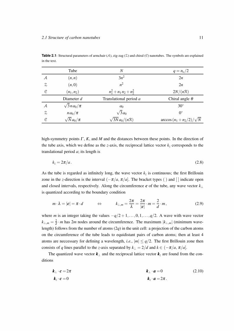
Figure 2.4: Brillouin zone of a (7,7) armchair and a (13,0) zig-zag tube (thick lines). The background is a contour
plot of the electronic band structure of graphene (white indicates the maximum energy). The graphene Brillouin
zone in the right panel is rotated by 30. The Brillouin zone consists of 2n (i.e., 14 and 26, respectively) lines
parallel to kz, where kz is the reciprocal lattice vector along the tube axis. Each line is indexed by m ∈ [−n,n],where m = 0 corresponds to the line through the graphene Γ point (k = 0). Note that the Brillouin-zone boundary
π/a is given by π/a0 for armchair and π/√
3a0 for zig-zag tubes. It can be seen from the symmetry of the graphite
hexagonal Brillouin zone that lines with index m and −m are equivalent. The same holds for k and −k with the
same index m.
This yields
kkk⊥ =2n1 + n2
qnRkkk1 +
2n2 + n1
qnRkkk2 (2.11)
kkkz = − n2
qkkk1 +
n1
qkkk2 . (2.12)
In Fig. 2.4 the Brillouin zones of a (7,7) armchair and a (13,0) zig-zag tube are shown for
m ∈ [−n,n] in relation to the graphene Brillouin zone. The line through the graphene Γ point
has the index m = 0. The position of the lines with m = 0 and m = n is the same for all zig-zag
and all armchair tubes, respectively, independent of their diameter. With increasing diameter
the number of lines increases while their distance decreases. For chiral tubes, see Fig. 2.8.
To a first approximation, the properties of carbon nanotubes are related to those of graphite
by taking from graphene the lines that correspond to the nanotube Brillouin zone, according to
Eqs. (2.11) and (2.12). For example, the electronic band structure of a particular nanotube is
found by cutting the two-dimensional band structure of graphene (see background of Fig. 2.4)
into q lines of length 2π/a and distance 2/d parallel to the direction of the tube axis. This
approach is called zone folding and is commonly used in nanotube research. Since the zone-
2.2 Symmetry of single-walled carbon nanotubes 13
Figure 2.5: Scanning tunneling microscopy images of an isolated semiconducting (a) and metallic (b) single-
walled carbon nanotube on a gold substrate. The solid arrows are in the direction of the tube axis; the dashed line
indicates the zig-zag direction. Based on the diameter and chiral angle determined from the STM image, the tube
in (a) was assigned to a (14,−3) tube and in (b) to a (12,3) tube. The semiconducting and metallic behavior of the
tubes, respectively, was confirmed by tunneling spectroscopy at specific sites. From Ref. [17].
folding procedure, however, neglects any effects of the cylinder geometry and curvature of the
tube walls, results obtained by zone folding have to be used with great care.
Experimentally, the atomic structure of carbon nanotubes can be investigated either by
direct imaging techniques, such as transmission electron microscopy [2,52] and scanning probe
microscopy [17,19,53–58], or by electron diffraction [59–62], i.e., imaging in reciprocal space.
Scannig tunneling microscopy (STM) offers measurements with atomic resolution, see Fig. 2.5.
From both, STM and electron diffraction, the chiral angle and tube diameter can be determined,
and hence the chiral vector (n1,n2), in principle, can be found experimentally. Interpretation
of the images is, however, delicate and often requires computations of the images and cross-
checking with other experimental results.
2.2 Symmetry of single-walled carbon nanotubes
The symmetry of carbon nanotubes is described by the so-called line groups, which were in-
troduced by Damnjanovic et al. [28–30, 63, 64]. Line groups are the full space groups of
one-dimensional systems including translations in addition to the point-group symmetries like
rotations or reflections. Therefore, they provide a complete set of quantum numbers. Damn-
janovic et al. [46,47,65] showed that every nanotube with a particular chirality (n1,n2) belongs
to a different line group. Only armchair and zig-zag tubes with the same n belong to the same
symmetry group. Moreover, starting from a single carbon atom, the successive application of
all symmetry operations of the group constructs the whole tube. Because the relation between
the carbon atoms and the symmetry operations is one-to-one, the nanotubes can be viewed as
2.2 Symmetry of single-walled carbon nanotubes 14
a realization of the line groups. Here we present the basic concepts of line groups and their
application in carbon nanotube physics.
2.2.1 Symmetry operations
In order to find the symmetry groups of carbon nanotubes, the symmetry operations of graphene
are considered [46, 65]. Those that are preserved when the graphene sheet is rolled into a
cylinder form the nanotube symmetry group. Translations by multiples of a of the graphene
sheet parallel to aaa remain translations of the nanotube parallel to the tube axis, see Fig. 2.2.
They form a subgroup TTT containing the pure translations of the tube. Translations parallel to
the circumferential vector ccc (perpendicular to aaa) become pure rotations of the nanotube about
its axis. Given n graphene lattice points on the chiral vector ccc, the nanotube can be rotated
by multiples of 2π/n. Single-walled nanotubes thus have n pure rotations in their symmetry
group, which are denoted by Csn (s = 0,1, . . . ,n− 1). These again form a subgroup CCCn of the
full symmetry group.
Translations of the graphene sheet along any other direction are combinations of transla-
tions in the aaa and the ccc direction. Therefore, when the graphene sheet is rolled up, they result
in translations combined with rotations about the nanotube axis. The order of these screw axis
operations is equal to the number q of graphene lattice points in the nanotube unit cell. They
are denoted by (Cwq |an/q)t with the parameter
w =q
nFr
[n
qR
(3−2
n1−n2
n1
)+
n
n1
(n1−n2
n
)ϕ(n1/n)−1]
. (2.13)
Fr[x] is the fractional part of the rational number x, and ϕ(n) is the Euler function [66]. On
the unwrapped sheet the screw-axis operation corresponds to the primitive graphene translationwq
ccc+ nqaaa. The nanotube line group always contains a screw axis; this can be seen from Eq. (2.6),
which yields q/n ≥ 2. In achiral tubes, q/n = 2 and w = 1, thus the screw axis operations in
these tubes consist of a rotation by π/n followed by a translation by a/2, see Fig. 2.2.
From the six-fold rotation of the hexagon about its midpoint only the two-fold rotation re-
mains a symmetry operation in carbon nanotubes. Rotations by any other angle do not preserve
the tube axis and are therefore not symmetry operations of the nanotube. This rotational axis,
which is present in both chiral and achiral tubes, is perpendicular to the tube axis and denoted
by U . In Fig. 2.6 the U -axis is shown in the (8,6), the (6,0), and the (6,6) nanotube. The U -axis
points through the midpoint of a hexagon perpendicular to the cylinder surface. Equivalent to
the U -axis is the two-fold axis U ′ through the midpoint between two carbon atoms.
Mirror planes perpendicular to the graphene sheet must either contain the tube axis (vertical
mirror plane σx) or must be perpendicular to it (horizontal mirror plane σh) in order to transform
2.2 Symmetry of single-walled carbon nanotubes 15
Figure 2.6: Mirror and glide planes and the two-fold rotational axes. Left: (8,6) nanotube with the U and U ′ axes.
As a chiral tube, it does not have mirror symmetries. Middle: (6,0) tube (zig-zag). Right: (6,6) tube (armchair).
The achiral tubes possess the horizontal rotational axes (U and U ′), the horizontal (σh) and the vertical (σx) mirror
planes (σx is in the Figure indicated as σv), the glide plane σx′ (σv′ ), and the roto-reflection plane σh′ . Taken from
Ref. [46].
the nanotube into itself. Only in achiral tubes the vertical and horizontal mirror planes, σx
and σh, are present [46], see Fig. 2.6. They contain the midpoints of the graphene hexagons.
Additionally, in achiral tubes the vertical and horizontal planes through the midpoints between
two carbon atoms form vertical glide planes (σx′ ) and horizontal roto-reflection planes (σh′)
(Fig. 2.6).
In summary, the general element of any carbon-nanotube line group is denoted as
l(t,u,s,v) = (Cwq |
an
q)t Cs
nUu σ vx , (2.14)
with t = 0,±1, . . . ;
s = 0,1, . . . ,n−1;
u = 0,1;
v =
0,1 achiral
0 chiral
and w,n,q as given above. Note that σh =Uσx. The elements in Eq. (2.14) form the line groups
LLL, which are given by the product of the point groups DDDn and DDDnh for chiral and achiral tubes,
respectively, and the axial group TTT wq :
LLLAZ = TTT 12nDDDnh = LLL2nn/mcm (armchair and zig-zag) (2.15)
Here 2π w/q determines the screw axis of the axial group. The international notation is in-
cluded for a reference to the Tables of Kronecker Products in Refs. [63] and [64].2
For many applications of symmetry it is not necessary to work with the full line group.
Instead, the point group is sufficient. For example, electronic and vibrational eigenfunctions at
the Γ point always transform as irreducible representations of the isogonal point group. For
optical transitions or first-order Raman scattering the point group is sufficient, because these
processes do not change the wave vector k. The point groups isogonal to the nanotube-line
groups, i.e., with the same order of the principal rotational axis, where the rotations include the
screw-axis operations, are
DDDq for chiral (2.17)
and DDD2nh for achiral tubes.
Since carbon-nanotube line groups always contain the screw axis, they are non-symmorphic
groups, and the isogonal point group is not a subgroup of the full symmetry group. We will
consider this below in more detail when we introduce the quantum numbers.
After having determined the symmetry operations that leave the whole tube invariant, we
now investigate whether they leave a single atom invariant or not. Those that do form the
site symmetry of the atom and are called stabilizers; the others form the transversal of the
group [47]. In principle, a calculation for all carbon atoms in the unit cell can be restricted to
those atoms that by application of the transversal form the entire system. As an example we
show how the atomic positions of the tube can be obtained from a single carbon atom [46].
We start with an arbitrary carbon atom and apply the U -axis operation. The atom is mapped
onto the second atom of the graphene unit cell (hexagon). The n-fold rotation about the tube
axis then generates all other hexagons with the first atom on the circumference. The screw-
axis operations (without pure translations) map these atoms onto the remaining atoms of the
unit cell. Finally, translating all the atoms of the unit cell by the translational period a forms
the whole tube. Thus if we know for example the electronic wave function of the tube at the
starting atom, we know the wave function of the entire tube.
Just a single atom is needed to construct the whole tube by application of the symmetry
operations of the tube; such a system is called a single-orbit system. The line groups of chiral
tubes comprise, besides the identity element, no further symmetry operations but those that
have been used for the construction of the tube. Therefore, the stabilizer of a carbon atom in
chiral tubes is the identity element; its site symmetry is CCC1. In achiral tubes, on the other hand,
there are additional mirror planes σh and σx. Reflections in the σh plane in armchair tubes and
in the σx plane in zig-zag tubes leave the carbon atom invariant. Thus the site symmetry of
2In these references, the meanings of the symbols n and q in are interchanged.
2.2 Symmetry of single-walled carbon nanotubes 17
Table 2.2: Symmetry properties of armchair (A), and zig-zag (Z) and chiral (C) nanotubes. The symbols are ex-
plained in the text. From the position rrr000 of the first carbon atom the whole tube can be constructed by application
of the line-group symmetry operations, see Eq. (2.19).
Tube Line group Isogonal rrr000
point group
A (n,n) TTT 2nDDDnh DDD2nh LLL2nn/mcm (r0 , 2π3n
,0)
Z (n,0) TTT 2nDDDnh DDD2nh LLL2nn/mcm (r0 , πn, a0
2√
3)
C (n1,n2) TTT rqDDDn DDDq LLLqp22 (r0 ,2π n1+n2
2N, n1−n2
2√
3Na0)
the carbon atoms in achiral tubes is CCC1h. We will see later that the higher site symmetry of
achiral nanotubes imposes strict conditions on their phonon eigenvectors and electronic wave
functions.
Using the symmetry operations of the tube, the atomic positions rrr in the unit cell can be
easily found. The position of the first carbon atom is defined at 13(aaa111 + aaa222) and the U -axis
is chosen to coincide with the x-axis. Then in cylindrical coordinates the position of the first
carbon atom in the nanotube is given by [46]
rrr000 = (r0,Φ0,z0) = (d/2 ,2πn1 + n2
2N,
n1−n2
2√
3Na0), (2.18)
where 2N = nqR = 2(n21 + n1n2 + n2
2). An element (Cwq |na
q)tCs
nUu acting on the atom maps it
onto the new position
rrrtsu = (Cwtq Cs
nUu|t na
q)rrr000
=
[d/2 ,(−1)uΦ0 + 2π
(wt
q+
s
n
),(−1)uz0 +
tn
qa
], (2.19)
where u = 0,1, s = 0,1, . . . ,n− 1, and t = 0,±1,±2, . . .. With the help of Eq. (2.19), the po-
sitions of all carbon atoms can be constructed for any nanotube. We summarize the symmetry
properties in Table 2.2.
2.2.2 Symmetry-based quantum numbers
A given symmetry of a system always implies the conservation law for a related physical quan-
tity. Well-known examples in empty space are the conservation of linear momentum caused by
the translational invariance of space or the conservation of the angular momentum (isotropy of
space). The rotational symmetry of an atomic orbital reflects the conserved angular-momentum
quantum number. The most famous example in solid-state physics is the Bloch theorem, which
2.2 Symmetry of single-walled carbon nanotubes 18
states that in the periodic potential of the crystal lattice the wave functions are given by plane
waves with an envelope function having the same periodicity as the crystal lattice.
Likewise, any quasi-particle of the nanotube or a particle that interacts with it “feels” the
nanotube symmetry. The state of the (quasi-) particle then corresponds to a particular repre-
sentation of the nanotube line group, i. e., its wave function is transformed in the same way by
the symmetry operations as the basis functions of the corresponding representation. Using this,
we can calculate selection rules for matrix elements, according to which a particular transition
is allowed or not. The probability for a transition from state |α〉 to state |β 〉 via the interaction
X is only non-zero, if |X |α〉 and 〈β | have some components of their symmetry in common.
If they do not share any irreducible component, their wave functions are orthogonal and the
matrix element 〈β |X |α〉 vanishes [67–70]. X can be, e.g., the dipole operator of an optical
transition.
In the next section we describe the irreducible representations of the carbon-nanotube line
groups in more detail. Here, we first introduce two types of quantum numbers to characterize
the quasi-particle states in carbon nanotubes and show their implications for conservation laws.
We start by describing the general state inside the Brillouin zone by the quasi-linear mo-
mentum k along the tube axis and the quasi-angular momentum m. The first corresponds to
the translational period; the latter to both the pure rotations and the screw-axis operations [47].
These states |k m〉 are shown by the lines forming the Brillouin zone, as depicted in Fig. 2.4 for
achiral tubes. For k = 0,π/a and m = 0,n the state is additionally characterized by its even or
odd parity with respect to the U -axis. Achiral tubes have additionally the parity with respect
to the vertical and horizontal mirror planes. k is a fully conserved quantum number, since it
corresponds to the translations of the tube, which by themselves form a group TTT . In contrast,
m arises from the isogonal point group DDDq, which is not a subgroup of the nanotube line group.
Therefore, m is not fully conserved and care has to be taken when calculating selection rules.
As long as the process remains within the first Brillouin zone (−π/a,π/a] for achiral tubes and
within the interval [0,π/a] for chiral tubes, m can be regarded as a conserved quantum number.
But if the Brillouin zone boundary or the Γ point is crossed, m is no longer conserved. Such a
process is often called an Umklapp process.
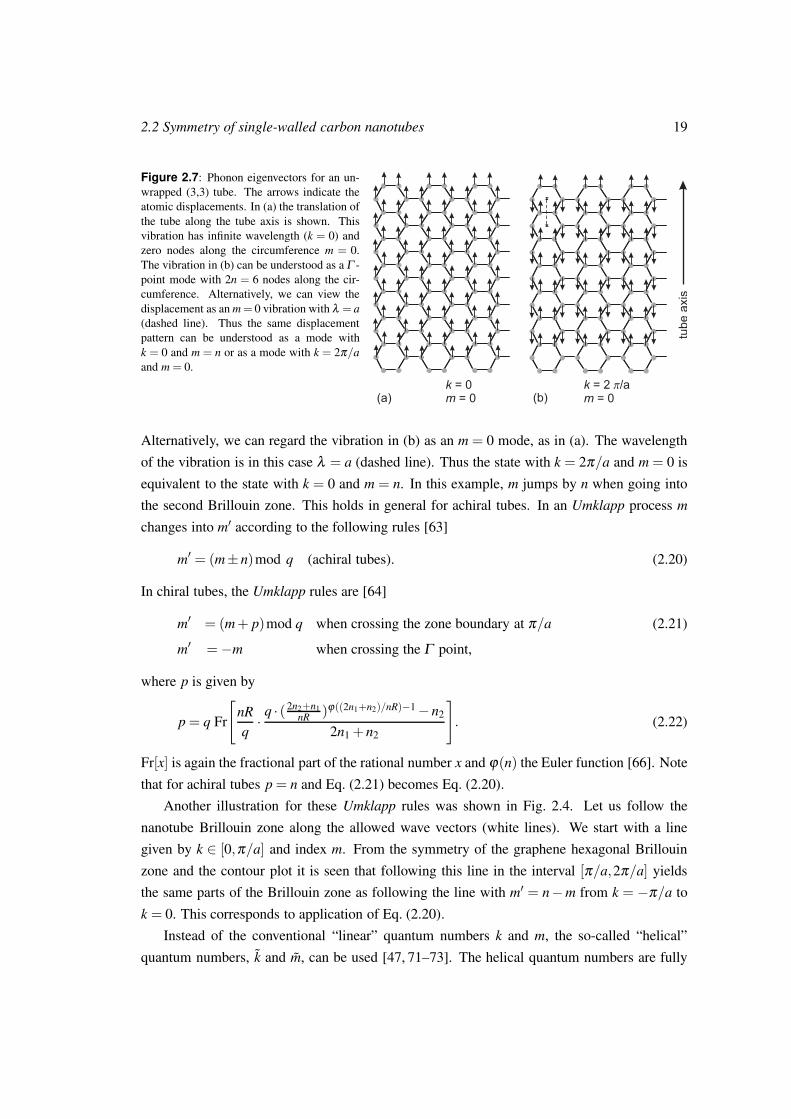
The change of m in Umklapp processes is illustrated in Fig. 2.7. A graphene rectangle is
shown, which is an unrolled (3,3) tube. The arrows indicate the displacement vectors of the
atoms along the tube axis. In (a), the translation of the tube along the tube axis is shown.
This mode has infinite wavelength along the tube axis and along the circumference, i.e., k = 0
and m = 0. If we want to relate the displacement in (b) to the z-translation, we find two
solutions. First, if we view the displacement as a Γ -point mode, we find 2n = 6 nodes along
the circumference. The vibrational state in (b) is then characterized by k = 0 and m = n.
2.2 Symmetry of single-walled carbon nanotubes 19
Figure 2.7: Phonon eigenvectors for an un-
wrapped (3,3) tube. The arrows indicate the
atomic displacements. In (a) the translation of
the tube along the tube axis is shown. This
vibration has infinite wavelength (k = 0) and
zero nodes along the circumference m = 0.
The vibration in (b) can be understood as a Γ -
point mode with 2n = 6 nodes along the cir-
cumference. Alternatively, we can view the
displacement as an m = 0 vibration with λ = a
(dashed line). Thus the same displacement
pattern can be understood as a mode with
k = 0 and m = n or as a mode with k = 2π/a
and m = 0.
tube a
xis
km
= 2 /a= 0
p
(a) (b)km
= 0= 0
Alternatively, we can regard the vibration in (b) as an m = 0 mode, as in (a). The wavelength
of the vibration is in this case λ = a (dashed line). Thus the state with k = 2π/a and m = 0 is
equivalent to the state with k = 0 and m = n. In this example, m jumps by n when going into
the second Brillouin zone. This holds in general for achiral tubes. In an Umklapp process m
changes into m′ according to the following rules [63]
m′ = (m±n)mod q (achiral tubes). (2.20)
In chiral tubes, the Umklapp rules are [64]
m′ = (m + p)mod q when crossing the zone boundary at π/a (2.21)
m′ =−m when crossing the Γ point,
where p is given by
p = q Fr
[nR
q· q · (
2n2+n1
nR)ϕ((2n1+n2)/nR)−1−n2
2n1 + n2
]. (2.22)
Fr[x] is again the fractional part of the rational number x and ϕ(n) the Euler function [66]. Note
that for achiral tubes p = n and Eq. (2.21) becomes Eq. (2.20).
Another illustration for these Umklapp rules was shown in Fig. 2.4. Let us follow the
nanotube Brillouin zone along the allowed wave vectors (white lines). We start with a line
given by k ∈ [0,π/a] and index m. From the symmetry of the graphene hexagonal Brillouin
zone and the contour plot it is seen that following this line in the interval [π/a,2π/a] yields
the same parts of the Brillouin zone as following the line with m′ = n−m from k = −π/a to
k = 0. This corresponds to application of Eq. (2.20).
Instead of the conventional “linear” quantum numbers k and m, the so-called “helical”
quantum numbers, k and m, can be used [47, 71–73]. The helical quantum numbers are fully
2.2 Symmetry of single-walled carbon nanotubes 20
conserved. In contrast to m, the new quantum number m corresponds to the pure rotations
of the nanotube, which form the subgroup DDDn of the nanotube-line group. Therefore, m is
fully conserved and takes n integer values in the interval (−n/2,n/2]. The screw-axis opera-
tions are incorporated in k, which can be considered as a “helical” momentum. Because the
screw-axis operations including pure translations form the subgroup TTT wq , k, too, is a conserved
quantum number in carbon nanotubes. The minimum roto-translational period is now nqa, and
k ∈ (−π/a, π/a], where π = π q/n. 3 In the Brillouin zone “BZ” defined by k,m there are
as many states as in the conventional Brillouin zone. The number of lines indexed by m is
reduced by a factor q/n, while the interval (−π/a,π/a] for k is extended by the same factor for
k. The linear and helical quantum numbers can be transformed into each other by the following
equations [74]
|k,m〉 = |k +wm
n
2π
a+ K
2π
a,m + Mn〉 (2.23)
|k,m〉 = |k− wm
n
2π
a+ K
2π
a,m−K p+ Mq〉 . (2.24)
Here, K, M, K, and M are integers determined by the condition that the quantum numbers are
in the intervals
k ∈ (−π
a,
π
a] m ∈ (−q
2,q
2] (2.25)
k ∈ (−q
n
π
a,q
n
π
a] m ∈ (−n
2,n
2]. (2.26)
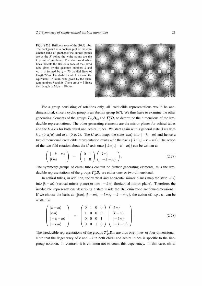
Figure 2.8 illustrates the relation between the “k,m” and the “k,m” quantum numbers for
a (10,5) tube. The number of atoms in the unit cell is 2q = 140; the linear quantum number
m ∈ (−q/2,q/2] takes q = 70 values. Thus the conventional Brillouin zone of the (10,5) tube
consists of 70 equidistant lines, which are depicted by the short solid white lines in Fig. 2.8.
Their direction is parallel to the tube axis, their length is 2π/a, where the translational period
a = 11.3A, and their distance is 2/d. The BZ indicated by the dashed white lines consists of
n = 5 lines indexed by m. Their length is 2qn
πa
= 28πa
. At k = 0 and m = 0 is the Γ point of
graphene, i.e., k = 0 and m = 0. We will see in Sects. 4.3 and 5.2 that for chiral tubes the helical
quantum numbers are much more helpful than the linear quantum numbers for, e.g., displaying
the phonon dispersion and using it in further calculations.
2.2.3 Irreducible representations
In this section we introduce the irreducible representations of the carbon-nanotube symmetry
groups. We shall explain the line-group notation used in Refs. [63] and [47], which, in contrast
to the more common molecular notation of crystal point groups, includes the full space group.
3Note that all intervals are defined modulo these intervals.
2.2 Symmetry of single-walled carbon nanotubes 21
Figure 2.8: Brillouin zone of the (10,5) tube.
The backgound is a contour plot of the con-
duction band of graphene; the darkest points
are at the K point; the white points are the
Γ point of graphene. The short solid white
lines indicate the Brillouin zone of the (10,5)
tube given by the quantum numbers k and
m; it is formed by q = 70 parallel lines of
length 2π/a. The dashed white lines form the
equivalent Brillouin zone given by the quan-
tum numbers k and m. There are n = 5 lines;
their length is 2π/a = 28π/a.
For a group consisting of rotations only, all irreducible representations would be one-
dimensional, since a cyclic group is an abelian group [67]. We thus have to examine the other
generating elements of the groups TTT 12nDDDnh and TTT w
q DDDn to determine the dimensions of the irre-
ducible representations. The other generating elements are the mirror planes for achiral tubes
and the U -axis for both chiral and achiral tubes. We start again with a general state |k m〉 with
k ∈ (0,π/a) and m ∈ (0,q/2). The U -axis maps the state |k m〉 into | − k −m〉 and hence a
two-dimensional irreducible representation exists with the basis |k m〉, |−k −m〉. The action
of the two-fold rotation about the U -axis onto |k m〉, |− k −m〉 can be written as
(|− k −m〉|k m〉
)=
(0 1
1 0
)(|k m〉|− k −m〉
). (2.27)
The symmetry groups of chiral tubes contain no further generating elements, thus the irre-
ducible representations of the groups TTT wq DDDn are either one- or two-dimensional.
In achiral tubes, in addition, the vertical and horizontal mirror planes map the state |k m〉into |k −m〉 (vertical mirror plane) or into | − k m〉 (horizontal mirror plane). Therefore, the
irreducible representations describing a state inside the Brillouin zone are four-dimensional.
If we choose the basis as |k m〉, |k −m〉, | − k m〉, | − k −m〉,, the action of, e.g., σx can be
written as
|k −m〉|k m〉|− k −m〉|− k m〉
=
0 1 0 0
1 0 0 0
0 0 0 1
0 0 1 0
|k m〉|k −m〉|− k m〉|− k −m〉
. (2.28)
The irreducible representations of the groups TTT 12nDDDnh are thus one-, two- or four-dimensional.
Note that the degeneracy of k and −k in both chiral and achiral tubes is specific to the line-
group notation. In contrast, it is common not to count this degeneracy. In this case, chiral
2.2 Symmetry of single-walled carbon nanotubes 22
tubes possess only non-degenerate representations and achiral tubes one- or two-dimensional
representations.
The examples given in Eq. (2.27) and Eq. (2.28) for chiral and achiral tubes, respectively,
apply to a state |k m〉 inside the Brillouin zone. At the Brillouin zone edges, on the other hand,
states with k and −k are the same; m and −m describe the same quantum number if m = 0 or
m = q/2. Then the dimension of the irreducible representation is reduced. Additionally, states
at the Brillouin-zone edges are characterized by parity quantum numbers with respect to the
U -axis and, in achiral tubes, to the mirror planes. The Umklapp rules, Eqs. (2.20) and (2.21),
are reflected by the fact that at the Brillouin zone boundaries the bands m are degenerate with
the bands m′ = (m+ p)modq [75]. An overview of the irreducible representations, degeneracy
as well as symmetry of polar and axial vectors and their symmetric and antisymmetric products
can be found in Ref. [75].
In the following we explain the line-group notation for the irreducible representations:
wave vector→ kXπm
←σh/ U-axis parity←m quantum number
↑ dimension (X = A,B,E,G) .
X is given by a letter that indicates the dimension of the representation: A and B are one-
dimensional, E two-dimensional, and G four-dimensional representations. For achiral tubes,
A and B give at the same time the parity quantum number with respect to the σx operation. A
corresponds to even and B to odd parity. In chiral tubes at k = 0, the subscript + or − denotes
even or odd parity under the U -axis operation and, in achiral tubes, under the σh operation.
For example, in achiral tubes 0B−0 is the one-dimesional irreducible representation of a Γ -point
state (k = 0) with zero nodes around the circumference (m = 0). This state has odd parity under
both the vertical (B) and the horizontal (−) reflections. In chiral tubes, kE2 denotes a two-fold
degenerate (E) state inside the Brillouin zone, i.e., k 6= 0 and k 6= π/a, with 4 nodes around
the circumference (m = 2). This state has no defined parity under rotation about the U -axis. A
summary of all irreducible representations of chiral and achiral carbon nanotubes is given in
Tables A1 and A2 of Ref. [47].
The irreducible representations at k = 0 can be related to the more common molecular
notation [76] of the corresponding isogonal point groups D2nh and Dq. In chiral tubes, 0A+0
is the fully symmetric representation A1; 0A−0 possesses odd parity under the U -axis operation
and therefore corresponds to A2 in the molecular notation. For m = q/2, the states have odd
parity under rotation by 2π/q about the principal axis, thus the representations 0A+q/2
and 0A−q/2
translate into B1 and B2, respectively. The degenerate representations 0Em are the same in the
molecular notation (Em).
Achiral tubes possess a center of inversion, thus the fully symmetric representation 0A+0 is
A1g in molecular notation; 0A−0 is A2u. The correspondence of the degenerate representations
2.2 Symmetry of single-walled carbon nanotubes 23
Table 2.3: Correspondence of the line-group notation for achiral tubes (LLLA,Z) at the Γ -point to the molecular
notation for the isogonal point group D2nh. For chiral tubes, the subscripts “g” and “m” are omitted; n is replaced
by q/2.
0A+0 0A−0 0B+
0 0B−0 0A+n 0A−n 0B+
n 0B−n 0E+±m 0E−±m
A1g A2u A2g A1u n even: B1g B2u B2g B1u m even: Emg Emu
n odd: B2u B1g B1u B2g m odd: Emu Emg
0E±m to Emg or Emu depends on whether m is even or odd. For example, we consider the
representation 0E−1 . The inversion of the achiral tube is given by the symmetry operation
σhCn2n. The character of 0E−1 for the inversion is therefore −2 cos (nm2π/q) = +2. Thus 0E−m
transforms into Emg if m is odd. We summarize the relationship between the line-group and the
molecular notation in Table 2.3. For chiral tubes, the subscripts “g” and “m” are omitted; n is
replaced by q/2.
Finally, we want to give an example of the use of the line-group symmetry to calculate se-
lection rules. We consider optical absorption in carbon nanotubes in the dipole approximation.
The momentum operator has the same symmetry as a polar vector. The z-component of a polar
vector in an achiral nanotube belongs to a non-degenerate represenation. It has even parity
with respect to the vertical mirror plane σx and odd parity under σh. Therefore, it transforms
as the irreducible representation 0A−0 . The x- and y-components are degenerate and have even
parity with respect to σh, therefore given by 0E+±1 [30]. In the dipole approximation, an optical
transition between the states |i〉 and | f 〉 is allowed if the representations of the polar vector and
of the electronic states have a common component:
D| f 〉⊗Dpv⊗D|i〉 ⊇ 0A+0 . (2.29)
This can be evaluated in the standard way by using the character tables in Refs. [64] and
[63]. More elegant and much faster, however, is the direct inspection of the quantum numbers.
Because of its 0A−0 symmetry, z-polarized light can change neither m (∆m = 0), nor the σx
parity (A). But since it carries a negative σh parity quantum number, it changes the σh parity
of the quasi-particle it interacts with. Similarly, x/y-polarized light changes the m quantum
number by ∆m = ±1, but leaves the σh parity unchanged. For example, the electronic bands
crossing at the Fermi level in armchair tubes (see Chap. 3) possess kEAn and kEB
n symmetry.
Between these two bands, an optical transition with z-polarized light (∆m = 0) is forbidden,
because it cannot change the σx parity of the electronic states from A to B.
2.3 Summary 24
2.3 Summary
In this chapter we showed how to construct the atomic structure and the reciprocal lattice of
carbon nanotubes from a given chiral vector (n1,n2). Single-walled carbon nanotubes have
line-group symmetry [46], i.e., they possess a translational periodicity only along the tube axis.
Within the concept of line groups, any state of a quasi-particle can be characterized by a set
of quantum numbers consisting of the linear momentum k, the angular momentum m, and, at
special points in the Brillouin zone only, parity quantum numbers. Only achiral tubes possess
additional vertical and horizontal mirror planes. When crossing the boundaries of the Brillouin
zone in a scattering process, special Umklapp rules apply, because m is not a fully conserved
quantum number. Alternatively, a different set of quantum numbers can be used, the so-called
helical quantum numbers. The notation and the application of the line-group symmetry for
calculating selection rules are explained.
3 Electronic band structure
In resonant Raman scattering one or more of the electronic transitions are real, and the Raman
signal is strongly enhanced. Thus the Raman intensity and, as we will show in Chap. 5 for
double-resonant scattering, also the Raman frequency depend sensitively on the electronic band
structure. In this chapter we summarize the basic properties of the carbon nanotube band
structure, as we will use them in Chap. 5 for the calculation of the Raman spectra.
Carbon nanotubes can be metallic or semiconducting. The simplest argument for that is
given by the zone-folding approach (Sect. 2.1), where the nanotube bands are obtained by
cutting the graphene bands according to the allowed wave vectors: In graphene, the conduc-
tion and valence bands cross the Fermi level at singular points, the K points in the Brillouin
zone [77]. Therefore, the tube is metallic, if the allowed states of the nanotube (Fig. 2.4) contain
the graphite K point, otherwise it is semiconducting [31]. For example, in all armchair tubes
the band with m = n includes the K point, thus they are always metallic. In general, the tubes
with chiral index (n1,n2) such that (n1−n2)/3 is integer, are metallic in this approximation.
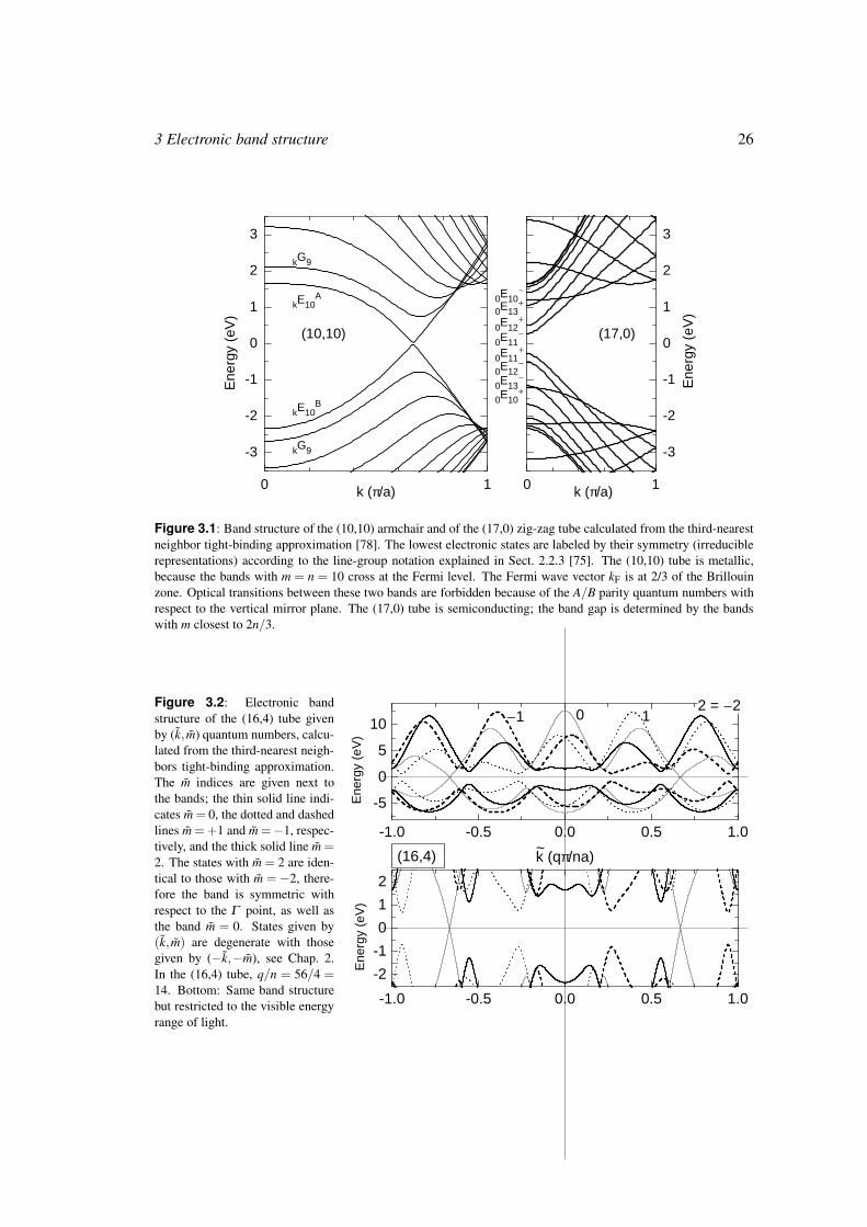
Figure 3.1 shows the band structures of the (10,10) and the (17,0) tube, obtained by zone
folding of the graphene π and π∗ bands. These were calculated within the tight-binding ap-
proximation including third-nearest neighbors, where the parameters were fit to the bands from
ab-initio calculations in the visible range of transition energies [78]. The (10,10) tube is metal-
lic with the Fermi wave vector kF at 2/3 of the Brillouin zone; the (17,0) tube is semiconducting.
The bands near the Fermi level are labeled by their symmetry (for the (17,0) tube the Γ -point
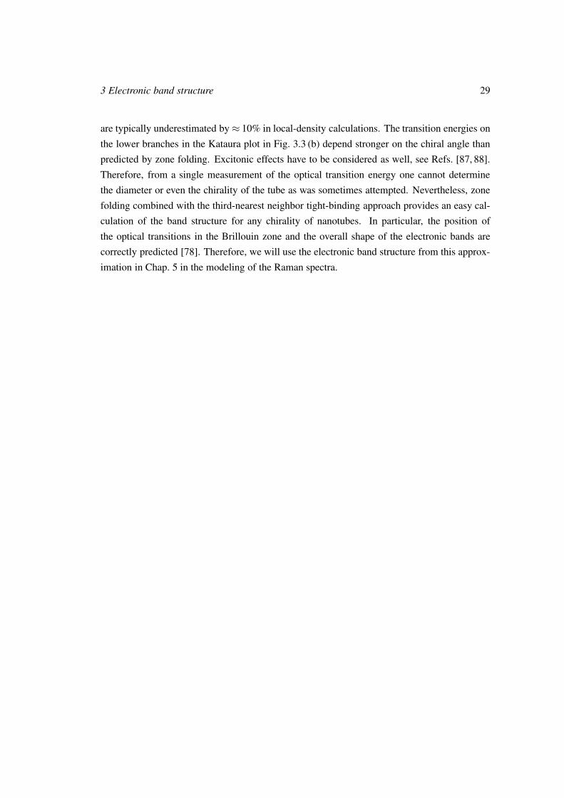
symmetry) [47, 75]. As an example for a chiral tube we show the band structure of the (16,4)
tube in Fig. 3.2. The bands are given by the helical (k,m) quantum numbers. The (16,4) tube
is metallic as well in this approximation, again with the Fermi wave vector at 2/3 of the helical
Brillouin zone. In general, the Fermi wave vector or, in semiconducting tubes, the wave vector
of the lowest transition energies is at the Γ point in tubes with R = 1 and at 2/3 of the Brillouin
zone in R = 3 tubes [79].
The transition energies are to first approximation proportional to the inverse tube diam-
eter [80, 81]. This is easily understood from the zone-folding approach, assuming linear,
isotropic bands at the graphite K point. Since the distance between two lines of the nano-
3 Electronic band structure 26
0 1
-3
-2
-1
0
1
2
3
kG9
kG9
kE10B
kE10A
(10,10)
Ene
rgy
(eV
)
k (π/a) 0 1
-3
-2
-1
0
1
2
3
0E10+
0E13-
0E12-
0E11+
0E10-
0E13+
0E12+
0E11-
(17,0)
Ene
rgy
(eV
)
k (π/a)
Figure 3.1: Band structure of the (10,10) armchair and of the (17,0) zig-zag tube calculated from the third-nearest
neighbor tight-binding approximation [78]. The lowest electronic states are labeled by their symmetry (irreducible
representations) according to the line-group notation explained in Sect. 2.2.3 [75]. The (10,10) tube is metallic,
because the bands with m = n = 10 cross at the Fermi level. The Fermi wave vector kF is at 2/3 of the Brillouin
zone. Optical transitions between these two bands are forbidden because of the A/B parity quantum numbers with
respect to the vertical mirror plane. The (17,0) tube is semiconducting; the band gap is determined by the bands
with m closest to 2n/3.
Figure 3.2: Electronic band
structure of the (16,4) tube given
by (k, m) quantum numbers, calcu-
lated from the third-nearest neigh-
bors tight-binding approximation.
The m indices are given next to
the bands; the thin solid line indi-
cates m = 0, the dotted and dashed
lines m = +1 and m =−1, respec-
tively, and the thick solid line m =2. The states with m = 2 are iden-
tical to those with m = −2, there-
fore the band is symmetric with
respect to the Γ point, as well as
the band m = 0. States given by
(k, m) are degenerate with those
given by (−k,−m), see Chap. 2.
In the (16,4) tube, q/n = 56/4 =14. Bottom: Same band structure
but restricted to the visible energy
range of light.
-1.0 -0.5 0.0 0.5 1.0
-5
0
5
10
(16,4)
2 = -2-1 10
~
Ene
rgy
(eV
)
k (qπ/na)
-1.0 -0.5 0.0 0.5 1.0
-2
-1
0
1
2
Ene
rgy
(eV
)
3 Electronic band structure 27
6 8 10 12 14
0
1
2
3
(b)(a)
E22S
E11S
Tra
nsiti
on e
nerg
y (e
V)
Diameter (Å)
6 8 10 12 14
1.5
2.0
2.5
(13,1)
(12,0)
(10,1)
(9,0)
(12,1)
(11,0)
(9,1)
(8,0)
Tra
nsiti
on e
nerg
y (e
V)
Diameter (Å)
Figure 3.3: Transition energies of carbon nanotubes as a function of diameter (so-called Kataura plot [82]) from
a third-nearest neighbor tight-binding calculation. Closed symbols indicate semiconducting tubes; open circles are
metallic tubes. ES11 and ES
22 are the first and second transitions in semiconducting tubes, respectively. (a) The
transition energies follow roughly a 1/d dependence, where the systematic deviations from this behavior increase
with smaller diameter and with increasing excitation energy. (b) Enlarged part of ES22 and EM
11 from (a). The lines
connect nanotubes with (n′1,n′2) = (n1−1,n2 +2); the chiral indices of the tubes at the outermost position on the
lower side of the semiconducting and of the metallic families are given. The lower branches of the ES22 transitions
consist of the tubes with (n1−n2)mod 3 =−1, the tubes in the upper branches have (n1−n2)mod 3 = +1.
tube Brillouin zone is 2/d, the energies obtained by cutting the graphene bands for different
tubes increase linearly with the inverse diameter. Systematic deviations from the 1/d depen-
dence are seen when the three-fold symmetry of the bands around the K point is taken into
account (so-called trigonal warping, see also the contour plot of the graphene conduction band
in Fig. 2.4). These deviations are even stronger if graphene bands obtained from ab-initio cal-
culations or tight-binding results including third-nearest neighbors interaction [78] are used in
the zone-folding procedure. The third-nearest neighbor tight binding results agree throughout
the Brillouin zone much better with the ab-initio calculation in the local-density approximation
than the usual nearest-neighbors tight-binding expression [78].
We show in Fig. 3.3 the transition energies obtained from the third-nearest neighbor tight-
binding approach as a function of tube diameter. Such a plot, usually shown for the simple
nearest-neighbor approximation, is commonly referred to as a Kataura plot [82]. Filled and
open circles indicate semiconducting and metallic tubes, respectively. The energies form v-like
branches below and above the 1/d line, as can be seen clearly in (b). The lines connect tubes
with (n′1,n′2) = (n1− 1,n2 + 2), where the zig-zag or small-chiral angle tubes are at the outer
positions. The chiral angle increases along such a branch towards the inner position; for the
metallic tubes, the inner tubes are of armchair type. For example, the branch starting with the
3 Electronic band structure 28
(9,0) tube consists of the (9,0), (8,2), (7,4), and (6,6) tube. Within the semiconducting ES22 tran-
sitions, the lower-branch tubes belong to the (n1− n2)mod 3 = −1 family, whereas the tubes
in the upper branches have (n1− n2)mod 3 = +1, and vice versa for the ES11 transitions. The
(n1−n2)mod 3 =±1 family reflects from which side of the K point the electronic bands result
in the zone-folding scheme. In the nanotubes with (n1− n2)mod 3 = −1 the first transition
(ES11) comes from between the Γ and K point, and the second transition (ES
22) from between
the K and M point. The opposite situation occurs for the (n1− n2)mod 3 = +1 nanotubes.
Since the dispersion of the electronic bands is different in the Γ -K and the K-M directions, this
results in systematic differences in the transition energy.
So far we did not include any effects of curvature, instead we treated the nanotube as a
flat rectangle from graphene with periodic boundary conditions. Blase et al. [83] first pointed
out that mixing and rehybridization of the π and σ orbitals in the curved graphite sheet can
significantly change the electronic band structure. These effects become particularly strong for
small-diameter nanotubes. For example, the (5,0) tube is metallic in contrast to what is ex-
pected from zone folding [84]. Moreover, the rehybridization effects as seen when comparing
ab-initio calculations with zone-folding results, are larger for zig-zag (small chiral angle) tubes
than for armchair tubes [85]. The deviation from the zone-folding bands is particularly large
for those transition energies that belong to the lower branches in Fig. 3.3 (b), and small for the
upper branches. This means that the lower branches are in fact bent downwards towards the
small-chiral angle tubes. Such a strong down-bending shape was recently confirmed experi-
mentally, where the transition energies were obtained by resonance Raman profiles [86], and
by photoluminescence excitation experiments [36–38].
A geometrical effect of the curvature is the small secondary gap opening at the Fermi
level in all chiral tubes that were above predicted to be metallic ((n1− n2)mod 3 = 0) [72,
79]. This can be understood from the structure of the curved graphite sheet, where the three
bonds between a carbon atom and its neighbors differ in length. Armchair tubes have still
a zero gap, if the geometry of the curved sheet is taken into account, but the Fermi wave
vector shifts [79]. Alternatively, the opening of the gap can be understood as a consequence of
symmetry: only in armchair tubes the two electronic states at the Fermi level possess different
quantum numbers, i.e., the A/B parity with respect to the vertical reflection, see Fig. 3.1. In
chiral tubes, in contrast, the vertical mirror planes are absent; both electronic states would have
the same quantum numbers. Therefore, an anti-crossing of the bands occurs, resulting in the
small gap at the Fermi level in chiral tubes; only armchair tubes are thus truly metallic.
In summary, the electronic band structure of carbon nanotubes can be reasonably well pre-
dicted by zone folding of the third-nearest neighbor tight-binding results, as is seen from the
good agreement with the ab-initio calculations. On the other hand, the excited electronic states
3 Electronic band structure 29
are typically underestimated by≈ 10% in local-density calculations. The transition energies on
the lower branches in the Kataura plot in Fig. 3.3 (b) depend stronger on the chiral angle than
predicted by zone folding. Excitonic effects have to be considered as well, see Refs. [87, 88].
Therefore, from a single measurement of the optical transition energy one cannot determine
the diameter or even the chirality of the tube as was sometimes attempted. Nevertheless, zone
folding combined with the third-nearest neighbor tight-binding approach provides an easy cal-
culation of the band structure for any chirality of nanotubes. In particular, the position of
the optical transitions in the Brillouin zone and the overall shape of the electronic bands are
correctly predicted [78]. Therefore, we will use the electronic band structure from this approx-
imation in Chap. 5 in the modeling of the Raman spectra.
4 Phonons in graphite and carbon
nanotubes
Phonons are the quasi-particles that describe the quantized lattice vibrations or normal modes
of a crystal. The crystal possesses 3N phonon branches where N is the number of atoms in the
unit cell. A three-dimensional crystal has three acoustic modes with zero frequency at the Γ
point, corresponding to uniform displacements of the crystal. All remaining branches, where
the atoms in the unit cell move out-of-phase, are referred to as optical phonons, since in polar
crystals they can directly couple to light [89]. Phonons are bosons and contribute the major
part to the heat capacity of a crystal. They play an important role for both transport and optical
properties, because they are main path by which excited electrons or other quasi-particles can
decay into lower energy states. In fact, in an ideal crystal at finite temperature phonons are the
only source of electrical resistance.
The knowledge of the phonon modes, of their dispersion and of the selection rules govern-
ing their interaction with other quasi-particles is therefore essential for a consistent understand-
ing of optical spectra and electrical transport characteristics. Information on the properties of
the phonons can be obtained from direct absorption of light by phonons (infrared spectroscopy,
for carbon nanotubes see Ref. [90,91]), measurements of the specific heat and the phonon den-
sity of states [92–94], Raman scattering (Chap. 5), or from transport experiments. In principle,
the phonon dispersion of a crystal can be measured by inelastic scattering of neutrons, elec-
trons, or X-ray photons. For these experiments, a minimum size of a single crystal is required,
which is not available from carbon nanotubes at present. The closest experimental approxima-
tion to the phonon dispersion of carbon nanotubes is therefore the in-plane phonon dispersion
of graphite.
Even in graphite the phonon dispersion was not known from experiments, because the
standard method of inelastic neutron scattered requires single crystals on the order of cm in
size, which do not exist. For the novel method of inelastic X-ray scattering, on the other hand,
single crystals ∼ 100 µm are sufficient. We describe the experimental technique of inelastic
X-ray scattering in Sect. 4.1 and present the experimental phonon dispersion of graphite in
4.1 Inelastic light scattering 31
Figure 4.1: Definition of the quasi-momenta in the inelastic scatter-
ing process. kkki and kkks are the wave vectors of the incoming and scat-
tered light, respectively. QQQ = qqq±HHH, where HHH is a reciprocal lattice
vector. The angle between kkki and kkks is defined as 2ϕ for convenience.
ki i, w
ks s, w
2f Q
Sect. 4.2. In Sect. 4.3 we discuss the phonon properties of carbon nanotubes, including their
relation to graphite, their symmetry and eigenvectors, and force-constants calculations of their
dispersion.
4.1 Inelastic light scattering
The dispersion relation of quasi-particles in a crystal can experimentally be determined from
the transfer of quasi-momentum and energy in an inelastic scattering process. For example, by
inelastic scattering of neutrons the phonon dispersion of many solids has been measured, such
as Si, Ge, GaAs, and diamond [95–99].
In the following we will discuss inelastic scattering of light by phonons to study the re-
lation between their wave vector qqq and energy hωph; the general principles apply to inelastic
scattering by other quasi-particles as well. In Fig. 4.1 we define the wave vectors kkki and kkks
of the incoming and scattered light, respectively, and the scattering wave vector (wave vector
transfer) QQQ = qqq±HHH, where HHH is a reciprocal lattice vector of the crystal. The conservation of
quasi-momentum and energy reads
kkki = kkks + qqq±HHH (4.1)
hωi = hωs± hωph , (4.2)
where the plus and minus sign, respectively, indicate the creation and annihilation of a phonon.
The magnitude |QQQ|= Q of the wave vector transfer is given by
Q2 = k2i + k2
s −2kiks cos (2ϕ) , (4.3)
where 2ϕ is the angle between kkki and kkks, see Fig. 4.1. If |kkki| ≈ |kkks|,
Q≈ 2ki sinϕ . (4.4)
This approximation applies to inelastic scattering of light by phonons: the phonon energy is
typically 1− 2 orders of magnitude smaller than the photon energy in the visible range. For
example, the longitudinal optical (LO) phonon in GaAs is at 36 meV, whereas the energy of
4.1 Inelastic light scattering 32
ki i, w ks s, w
2ff Q
ki i, wk’s s, w’
2 ’f
f’Q’
Figure 4.2: The magnitude of the momentum transfer is varied by changing the scattering angle 2ϕ . To conserve
the direction of the wave vector QQQ, the sample (indicated by the hexagon) has to be rotated by ∆2ϕ/2.
visible light is around 2.5 eV. Thus incoming and scattered light have almost the same energy
and therefore momentum. When changing the scattering angle 2ϕ by ∆(2ϕ) = 2ϕ ′− 2ϕ , the
magnitude of the scattering wave vector QQQ is varied, see Fig. 4.2. The direction of QQQ is kept the
same, if the sample is simultaneously rotated by ∆(2ϕ)/2. The maximum momentum transfer
is obtained for 2ϕ = 180 (backscattering geometry) with Q = 2ki.
In the visible range, inelastic scattering of light by phonons is called Raman scattering [100].
The wave vector of visible light ki = 2πn/λ is on the order of 5/102 nm−1 = 0.5× 10⁻² A−1
at λ = 500 nm in a material with refractive index n = 4. In contrast, the extension π/a of the
Brillouin zone, i.e., the range of phonon wave vectors, is typically ∼ 1 A−1. Therefore, the
maximum momentum transfer Q = 2ki is by about two orders of magnitude smaller than π/a,
and only Γ -point phonons (q≈ 0) can be probed by conventional Raman scattering.
In order to measure phonons from the entire Brillouin zone, either the photon energy (and
hence momentum) has to be increased by several orders of magnitude into the X-ray range
(∼ 10 keV), or higher-order Raman processes have to be studied. In higher-order Raman scat-
tering, two or more phonons are involved. Then the q≈ 0 rule can be fulfilled by two phonons
with large but opposite wave vector and q1 + q2 ≈ 0. Another higher-order process includes
elastic scattering by defects instead of scattering by a second phonon. Usually, however, it is
not possible to measure the phonon dispersion relation by higher-order scattering. All phonon
wave vectors contribute simultaneously to the spectra, and the second-order Raman spectra
resemble the phonon density of states [101]. An exception to this are resonant higher-order
Raman processes where particular phonon modes are enhanced, depending on the excitation
energy [102]. Such processes allow a mapping of the phonon dispersion and will be discussed
in detail in Chap. 5. Here we follow the first approach, i.e., first-order Raman scattering us-
ing X-rays for excitation, and present the measurement of the phonon dispersion relations in
graphite.
4.1 Inelastic light scattering 33
4.1.1 Inelastic X-ray scattering: experiment
Inelastic X-ray scattering for measuring phonon dispersion relations is a comparatively young
experimental technique. The first experiments were carried out about 15 years ago [103],
for a review see Ref. [104]. Although inelastic neutron scattering has been used for mea-
suring phonon dispersion relations for several decades already and become a standard tech-
nique [95, 96, 105, 106], there are several advantages of using X-rays instead of neutrons for
excitation. Inelastic X-ray scattering can be applied to relatively small samples, for example
for investigations under high pressure in a diamond anvil cell [107] or if only small amounts of
the sample are available.
One major challenge is the high energy resolution of ∆E/E ≈ 10 meV/10 keV= 10−6 that
is required in order to detect the inelastically scattered light only ∆E ∼ 10 meV apart from the
elastically scattered signal at∼ 10 keV and moreover to measure the typically flat dispersion of
optical phonons. This high resolution can achieved by using Bragg reflection in backscattering
geometry from single crystals for the main monochromators [103].
We performed the inelastic X-ray scattering at the beamline ID28 at the European Syn-
chrotron Radiation Facility. The experimental setup is schematically drawn in Fig. 4.3. The
white beam is first pre-monochromatized and then backscattered from a second, high-resolution
monochromator. The selected photon energy was 17794 eV. The monochromators are single
crystals of Si; in the present experiment we used the (999)-reflection plane for the backscat-
tering monochromator, resulting in an energy resolution of 3.1 meV. The energy difference
between incident and scattered light was scanned by changing the temperature of the main
monochromator. The temperature controls the lattice constant of the Si crystal and hence the
wavelength selected by the Bragg condition. Here, a temperature difference of 1 K between
main monochromator and analyzer corresponded to 46 meV energy difference between in-
coming and detected light. The advantage of this method of scanning the energy is that the
monochromator is not rotated and the energy resolution is constant. In contrast to common
Raman experiments the energy of the incoming light was varied, whereas the detection energy
was kept constant. The energy axis was calibrated by setting the energy transfer to zero at the
position of the Bragg peak. The beam can be focused by horizontal and vertical mirrors to a
spot size of 30× 60 µm2 in the sample. The 7 m long spectrometer arm was equipped with a
set of five analyzers, allowing the simultaneous detection from five different qqq vectors.
By rotating the spectrometer arm, the scattering angle 2ϕ is selected. The sample is
mounted on a goniometer head with the same vertical axis of rotation as the spectrometer
arm, allowing to vary the angle ϕ between a given direction in the sample and the incoming
beam. We show the selection of angles and wave vectors in Fig. 4.4 in more detail. In (a)
an elastic scattering process, i.e., Bragg reflection, is depicted in reciprocal space, using the
4.1 Inelastic light scattering 34
white beammirror
sample
detectormultilayerelement
analyzer
pre-mono-chromator
backscatteringmonochromator
monochromaticbeam
undulatorsource
Figure 4.3: Experimental setup of the inelastic X-ray scattering at beamline ID28 at the European Synchrotron
Radiation Facility. The monochromators select an energy of the incident beam of 17794 eV. The monochromatized
beam is focused by the multilayer element (horizontal) and a cylindrical mirror (vertical) onto the sample. Rotation
of the spectrometer arm and of the sample select the scattering wave vector QQQ and the phonon wave vector qqq.
The monochromators and analyzers are formed by Si crystals; the detectors are Peltier-cooled Si diodes. From
http://www.esrf.fr.
Ewald-construction [108, 109]. The dots indicate the reciprocal lattice of the crystal. In elastic
scattering, incoming and scattered wave vectors have the same magnitude. The wave vector
transfer QQQ is exactly a reciprocal lattice vector HHH, measuring in real space the distance between
the lattice planes perpendicular to HHH.
In Fig. 4.4 (b) an inelastic scattering process is shown, assuming again ki = ks for inelastic
X-ray scattering with phonons. The sample is rotated by an angle ϑ with respect to the incident
beam. If the spectrometer arm, i.e., the direction of kkks, is rotated by 2ϑ , the direction of the
wave vector transfer QQQ is the same as in (a), but it has now a smaller magnitude Q = H− q.
Thus inelastically scattered light is observed in the direction of kkks. Its energy difference with
respect to the incoming photon energy is equal to the phonon energy at wave vector qqq. Note
that the scattering angle “2ϕ” is not always twice the angle “ϕ” of the sample. For example, to
measure qqq ⊥ HHH in Fig. 4.4 (b), the scattering angle “2ϕ” has to be enlarged. If the change 2ϑ
in scattering angle, however, is twice the change ϑ in the angle of the sample, the direction of
a chosen scattering wave vector QQQ remains constant.
The amplitude of the inelastically scattered light is proportional to
where the sum is over the integer values m = 1, ...,(n− 1). In chiral (C) tubes, the dynamical
representation is decomposed into
DdynC
=3(A1 + A2 + B1 + B2)+ 6∑m
Em , (4.8)
where m takes integer values from (−n/2,n/2].
In contrast to three-dimensional crystals, the nanotube (like any one-dimensional crystal)
possesses four acoustic modes instead of three. These are the translations into three directions
and the rotation about the tube axis. The rotational mode, which becomes a twisting vibration
at finite wave vector, results from the translation of graphene along the chiral vector. The
symmetry of the acoustic modes is A2(u) for the z-translation, E1(u) for the xy-translation and
A2(g) for the rotational mode. The subscripts u and g apply to achiral tubes only.
4.3 Phonon dispersion of carbon nanotubes 45
The irreducible representations which transform like a polar vector determine the infrared-
active phonons. In the nanotube line groups, the z-component of the polar vector corresponds to
the non-degenerate A2(u) representation; the x- and y- components transform like E1(u). There-
fore, the infrared-active modes (after subtracting the acoustic modes) are [136]
infrared active: A2u + 2E1u (zig-zag)
3E1u (armchair)
A2 + 5E1 (chiral tubes). (4.9)
From the symmetric part of the direct product of two polar-vector representations, [(A2u ⊕E1u)⊗(A2u⊕E1u)], the symmetry of the Raman-active phonons is derived to be A1g + E1g + E2g
in achiral tubes and A1 + E1 + E2 in chiral tubes [30]. The Raman active modes in carbon
m = 0 changes into m = n for q ∈ (π/a,2π/a]. In chiral tubes, it is more convenient to use the
helical quantum numbers k,m; then the entire m = 0 band is allowed in (z,z) configuration.
In summary, the selection rules for large-q Raman scattering in carbon nanotubes are given
by the conservation of the quasi-angular momentum m. If q > π/a, the Umklapp rules must
be additionally applied. For m = 0 and m = n phonons in achiral tubes, the allowed modes are
further restricted by parity quantum numbers. In general, for q 6= 0 the selection rules are less
restrictive than for Γ -point phonons, since some of the parity quantum numbers are defined
only at q = 0. If a phonon mode is forbidden at the Γ point but allowed for q > 0, however,
continuity prevents the mode from having a large Raman signal at small q.
5.2 The D mode in carbon nanotubes
In Fig. 5.2 we saw already that the disorder-induced D mode of carbon nanotubes shifts signif-
icantly with excitation energy. This peculiar behavior is known for long from the D mode in
graphite [163–166]. The origin of the excitation-energy dependence in graphite was resolved
by Thomsen & Reich [133] as defect-induced, double-resonant Raman scattering. Laser-
energy dependent studies in carbon nanotubes first focused on the D mode as well, because
of its obvious correspondence to the graphite D mode and because the shift with laser energy
is an order of magnitude larger than the shift of the high-energy modes and therefore easier to
detect. The shift of the HEM frequencies will be studied in detail in Sect. 5.4. Here we discuss
the origin of the D mode in carbon nanotubes and show the correspondence and the differences
to graphite.
By applying the concept of defect-induced, double-resonant Raman scattering (Sect. 5.1),
the D-mode spectra of carbon nanotubes are found theoretically. As discussed in Sect. 5.1, the
double-resonance is determined by both electron and phonon dispersions. We make use of the
5.2 The D mode in carbon nanotubes 65
Figure 5.7: Electronic band
structure (top) and model phonon
dispersion (bottom) of an armchair
nanotube. The Fermi wave vector
kF is at 2/3 πa
in armchair tubes.
Resonant and non-resonant tran-
sitions are indicated by solid and
dashed arrows, respectively. Note
that the optical transition between
the bands crossing the Fermi level
(m = n) is forbidden by symmetry.
-2
0
2
n-2
n-1
n
n-2
n-1
n
-kF kF
2kFkF
D mode∆ m = 0
Ene
rgy
(eV
)
1300
1400
1500
1600
~m = 0
π/a
m = n
m = 0
G
G
2π/a
-π/a π/a P
hono
n fr
eque
ncy
(cm
-1 )
electronic band structure presented in Chap. 3 and the selection rules predicted by symmetry
(Sects. 2.2 and 5.1.1). For the phonons we will use model dispersions.
The scattering process of the D mode in armchair tubes is shown in Fig. 5.7 (top). For z-
polarized light, an electron-hole pair is excited in the band with m = n−1, near the Fermi wave
vector kF for visible light. In the zone-folding approach, the Fermi wave vector kF corresponds
to the K point of graphite. The electron is scattered across the Γ point within the same band by
a double-resonant phonon with qdr ≈ 2kF = 43
πa
. It is then scattered back elastically by a defect
and recombines with the hole (Sect. 5.1). Here the phonon must have mph = 0, because the
defects lead to a relaxation of the quasi-linear momentum conservation only; it cannot change
the quasi-angular momentum quantum number m, see Table 5.1.
In the lower part of Fig. 5.7 we give an example of a model phonon dispersion as the one
used in the calculations below. The required phonon wave vector qdr ≈ 2kF is larger than the
Brillouin zone. In this case, we have to apply the Umklapp rules Eq. (2.20):
2kF =4
3
π
a≡ 4
3
π
a− 2π
a=−2
3
π
a.
and
m′ = m + n = 0+ n = n
Thus in the conventional Brillouin zone the allowed phonon that leads to the D mode has a
wave vector qdr ≈ 2π/3a = kF and band index m = n in armchair tubes. In the extended or
5.2 The D mode in carbon nanotubes 66
1320
1340
1360
1380(10,10)
calc.
76 cm1/eV
42 cm1/eV
Sto
kes
shift
D m
ode
(cm1
)
2.0 2.2 2.4 2.6 2.8 3.0
1300
1320
1340
(a) (b)
exp.63 cm1/eV
SWNT 1.3 nm
47 cm1/eV
Excitation energy (eV)
1320 1350
λ = 466 nm
1350 1400
3.0 eV
2.6 eV
2.2 eV(11,11)
γ0= 2.9 eV
Inte
nsi
ty (
a.u
.)
Raman shift (cm1)
Figure 5.8: (a) D mode spectra calculated for the (11,11) tube [149]. The electronic band structure was calculated
by the first-neighbors tight-binding approximation with γ0 = 2.9 eV, and γ = 0.1 eV. The D-mode frequency clearly
depends on excitation energy. The intensity decreases with increasing laser energy. (b) D-mode frequency as
a function of excitation energy. Top: calculation for the (10,10) tube; bottom: experimental data from bundled
single-walled nanotubes with a mean diameter of 1.3 nm. The inset shows an experimental spectrum.
helical Brillouin zone, i.e., in the description by (k,m) quantum numbers, the phonon branch
with m = 0 is taken (dashed line in Fig. 5.7).
Both electron and phonon states relevant for the double-resonant D mode are derived from
the K point in graphite. Therefore, the double-resonant phonon corresponds to a K-point mode
and the observed frequency is similar to the D mode in graphite. For higher incoming laser
energy, the resonant optical transitions occur at larger distance from kF. Hence qdr is smaller
if the optical transition is on the left of the conduction-band minimum in Fig. 5.7 and larger
if the optical transition is on the right. In both cases, the double-resonant phonon wave vector
moves away from kF. This results in an increase of the phonon frequency with laser energy as
the phonon band m = n possesses a minimum at kF (or m = 0 at 2 kF).
The Raman spectra of the D mode, calculated according to the scattering process in Fig. 5.7,
are shown in Fig. 5.8 (a) for the (11,11) tube. The spectra show a clear dependence on laser en-
ergy. The Raman intensity decreases with increasing laser energy, because the electron density
of states is smaller for electron wave vectors away from kF. The D mode is not symmetric and
consists of two peaks, which shift at different rates. Several reasons account for this line shape.
The conduction band minimum is not exactly at kF = 2π/3a, the minimum is not symmetric,
and incoming and outgoing resonances have slightly different double-resonance conditions, see
also Fig. 5.5. The structure due to incoming and outgoing resonance is not resolved. In chiral
nanotubes, the peak structure can be even more complex due to several electronic bands con-
tributing simultaneously. In Fig. 5.8 (b) we show the frequency of the D mode as a function of
laser energy. The calculated shifts for a (10,10) tube (42 and 76 cm−1/eV) agree well with the
5.2 The D mode in carbon nanotubes 67
experiment on SWNT bundles (47 and 63 cm−1/eV). The experimental spectrum in the inset
shows that the D mode is not a single line but indeed contains at least two peaks.
Comparing tubes of the same chiral angle with different diameter, we find that at low
excitation energy the absolute D-mode frequency is lower for smaller tubes but the rate by
which the D mode shifts is larger. This is understood from the scattering process shown in
Fig. 5.7. A smaller diameter results in a larger separation of conduction and valence bands.
At the same laser energy, the wave vector of the excited electron is closer to kF and hence
the phonon frequency is lower than in larger-diameter tubes. Since the slope of the electron
bands is smaller near kF, the same variation in laser energy results in a larger change of the
excited-electron wave vector. Therefore, the change of the double-resonant phonon wave vector
and hence the frequency shift is larger. The predicted diameter dependence of the D-mode
frequency was observed in experiments on isolated tubes and bundles [44, 167, 168].
In the above discussion we showed that both the electron and phonon wave vectors that are
involved in D-mode scattering correspond to the Fermi wave vector kF (K point in graphite).
Therefore, they are approximately the same. Simultaneously, the double-resonant phonon wave
vector qdr is about twice the electron wave vector. Only if the electron wave vector is at 2/3 of
the Brillouin zone, it is equal to the phonon wave vector qdr ≈ |2kF− 2πa|= 2π
3a. This condition,
i.e., kF = 2π/3a, is only fulfilled in R = 3 tubes, see Ref. [79] and Chap. 3. A strong D-mode
scattering and a systematic excitation-energy dependence thus cannot be observed in R = 1
tubes [149]. Consequently, a weak Raman signal in the D-mode region does not necessarily
indicate fewer defects in the investigated nanotubes but can be due to the presence of R = 1
tubes. On the contrary, a strong D mode and a systematic shift with laser energy is an indication
of metallic tubes.4 This prediction is based on the assumption that only phonons with m = 0
(and, including Umklapp processes, m = 0) are allowed by symmetry. If elastic scattering by
the defect could change the quasi-angular momentum m as well – which is unlikely – the D
mode would be double-resonant for any chirality [169].
As an example of a chiral R = 3 tube we calculated the D mode of the (8,2) tube. The elec-
tronic band structure given by helical quantum numbers is shown in Fig. 5.9. As for armchair
tubes, the optical transitions occur near 2/3 of the (helical) Brillouin zone, and the double-
resonant phonon wave vector qdr ≈ 43
πa
, where π = qπ/na, see Chap. 2. The resulting D-mode
spectra are shown in Fig. 5.10. The main peak shifts by 40 cm−1/eV.
Above we showed that a strong D-mode scattering with a systematic excitation-energy
dependence cannot not occur in R = 1 tubes. In second-order overtone scattering, on the
other hand, the condition mph = 0 has to be fulfilled only by the sum of both phonons, mph =
4All tubes with R = 3 are metallic; semiconducting tubes always have R = 1. Only a small fraction of metallic
tubes has R = 1, among them all metallic zig-zag tubes.
5.2 The D mode in carbon nanotubes 68
-1.0 -0.5 0.0 0.5 1.0
-5
0
5 ~
~m = 1
m = 0
-kF kF
(8,2)
D mode
Ene
rgy
(eV
)
k (qπ/na)
Figure 5.9: Electronic band structure of the (8,2) tube calculated within the tight-binding approximation including
third-nearest neighbors. The visible range of optical transitions is shaded; the scattering process for the D mode is
indicated by arrows. Because the (8,2) tube has R = 3, the m = 0 conduction and valence bands cross the Fermi
level at kF = 2π/3a [79]. π = qπ/na = 14π/a, and m = 0,1. Scattering by phonons with m = 0 and q = 2kF leads
to the D mode.
mph,1 + mph,2 = 0, see Table 5.1. Thus the second-order D∗-mode becomes allowed in any
tube, if mph,1 = −mph,2 [170]. We will discuss this here for zig-zag nanotubes. Since zig-zag
tubes always have R = 1, i.e., the singularities in the joint density of states are at the Γ point,
D-mode scattering is not allowed for mdefect = 0. In Fig. 5.11 we show the electronic band
structure of the (17,0) tube near the Γ point. In (a) the defect-induced double-resonance in
(z,z)-polarization is displayed, leading to the first-order spectrum. Only phonons with mph = 0
are allowed. Since the double-resonant phonon wave vectors are rather close to the Γ point,
the scattering process in (a) yields Raman peaks in the range of the high-energy modes, see
Sect. 5.4. On the other hand, for Raman peaks in the D-mode range, phonons with m ≈ 2n/3
are required. In this case, the scattered electron with mb = ma + 2n/3 cannot recombine with
the hole (ma) in a z-polarized optical transition, and the D mode does not appear in the first-
Figure 5.10: D mode spectra of the
(8,2) tube. The phonon dispersion
was modeled by an analytical func-
tion; the broadening parameter was set
to γ = 0.05 eV. The main peak shifts
by 40 cm−1/eV and the smaller one by
27 cm−1/eV.
1380 1400 1420
2.88 eV2.54 eV
2.4 eV2.2 eV(8,2)
Ram
an In
tens
ity (
a.u.
)
Raman Shift (cm-1)
5.2 The D mode in carbon nanotubes 69
Figure 5.11: Electronic band
structure of the (17,0) tube near
the Γ point. The numbers indicate
the band indices m. The band ex-
trema are at the Γ point; the low-
est optical transitions occur in the
bands with m ≈ 2n/3. In achi-
ral tubes, the states with m and
−m are degenerate. (a) Double-
resonant scattering with an m =0 phonon and defect, resulting in
high-energy modes. (b) Double-
resonant scattering in second order
by two phonons with m = 12 and
m = −12, leading to the overtone
D∗ of the D mode.
-1
0
1 11 12
(a) 1112
∆m = 0
∆m = 0
12 11
Ene
rgy
(eV
)
(17,0)
Γ
(b) 1112
∆m = 0
-12
∆m = -12
∆m = +12
12-11 11
Γ
order spectrum of zig-zag tubes. In Fig. 5.11 (b) a second-order process is shown leading to the
D∗ mode. For example, if the electron-hole pair is excited in the ma = 11 band, a phonon with
mph = 12 scatters the electron to the band mb = (ma +mph)mod 2n = 11+12−34 =−11, see
Fig. 5.11 (b). A second phonon with mph =−12 scatters the electron back to near the original
band. Because of the σh parity quantum numbers of the states at the Γ point, phonons with even
parity are allowed only if |ma| and |mb| are both smaller or both larger than 2n/3, see Chaps. 2
and 3. Vice versa, if the phonon has σh =−1, one of the electronic states must have |m|> 2n/3
and the second one |m| < 2n/3. Taking into account these selection rules, we calculated the
D∗-mode spectra of the (19,0) tube in Fig. 5.12. The D∗ mode is in the expected frequency
range and shifts by ≈ 120 cm−1/eV, in reasonable agreement with experiments [171].
The double-resonance process as the origin of the D mode in graphite and carbon nanotubes
is well established and validated by experiments. Nevertheless, some interpretations attribute
the shift of the D mode in carbon nanotubes to the selective enhancement of different tubes in
Figure 5.12: D∗ Raman spectra calculated for the
(19,0) tube at different excitation energies [170].
The phonon dispersion was taken from the force-
constants calculations described in Sect. 4.3.2. The
shift with laser energy amounts to ≈ 120 cm−1/eV.
2650 2700 2750 2800
2.4 eV
2.2 eV2.0 eV
1.8 eV
(19,0)overtone scattering D*
Inte
nsity
(ar
b. u
nits
)
Raman Shift (cm-1)
5.2 The D mode in carbon nanotubes 70
Figure 5.13: D-mode frequency as a
function of laser energy measured on
isolated tubes on two different spots of
the sample (filled circles). The open tri-
angles are calculated values for the (8,8)
tube, where a model dispersion was used
for the phonons. The calculated D mode
is composed of two peaks; the upper one
agrees very well with the experiment.
In the experimental data, the individual
peaks were not resolved. For the spectra
see Fig. 5.25.1.6 1.8 2.0 2.2 2.4 2.6
1300
1320
1340
1360
Ram
an S
hift
(cm
-1 )
Excitation Energy (eV)
63 cm-1/eV (#1)
55 cm-1/eV (#2) calc. (8,8) tube
resonant Raman scattering [169, 172]. The D-mode frequency changes in this picture because
at a different excitation energy the Raman signal from a different tube is observed; a D-mode
shift in a single tube is not predicted, in contrast to the model explained above. Laser-energy-
dependent Raman measurements, however, showed that the D mode of an isolated tube is not
constant but shifts as in experiments on bulk samples. In Fig. 5.13 we present the D-mode
frequencies as a function of excitation energy in an isolated tube and a thin bundle [173], for
the measurements on isolated tubes see Sect. 5.4. The D mode shifts at a rate similar to that
observed in bundles, showing that the dependence on excitation energy indeed is the property
of a single tube and not an ensemble effect.
Finally, we want to comment on the phonon dispersion. In this section we always used
a model dispersion like the one in Fig. 5.7, that was adapted to the theoretically predicted
longitudinal (LO) branch in graphite. Although in armchair tubes the m = 0 LO branch is
actually forbidden because of its σx parity quantum number being odd (Chap. 4), we used it
in the calculations because it was the only one predicted with a minimum at about 1200−1300 cm−1. In chiral tubes, the σx parity quantum number does not exist, thus both LO and
TO branches are allowed. Meanwhile we found from inelastic X-ray scattering in graphite
(Chap. 4) that the TO branch was incorrectly predicted in most of the previous calculations. The
experiments showed that in fact the TO is at about the same frequencies as the LO was believed
to be. Therefore, the D mode in carbon nanotubes comes from the TO-derived phonon branch
instead from the LO, as well as the D mode in graphite. This is consistent with the selection
rules; for graphite we discuss the D mode, based on the new experimental data, in Sect. 5.3.
Since no revised calculations of the phonon dispersion in carbon nanotubes are available up
to now, we stayed with the model dispersions in this section. The implications of the double-
resonant model as well as the good qualitative agreement of the D-mode calculations with
Raman experiments are not affected by this correction, because just the name of the model
dispersions had to be altered.
5.3 The D mode in graphite 71
5.3 The D mode in graphite
We showed above for carbon nanotubes that the double-resonance model provides an excellent
understanding of all properties of the D mode. Nevertheless, the quantitative analysis so far
relied on partly arbitrary assumptions about the phonon dispersion; for example, model dis-
persions by simple analytical expressions were used in Fig. 5.8 and in Refs. [133, 149, 169].
Because the theoretically determined phonon dispersions of graphite and hence carbon nan-
otubes were contradictory in many respects, see Sect. 4.2, quantitative predictions of the D
mode were difficult to judge. For graphite, however, the experimental data of the phonon dis-
persion presented in Sect. 4.2 allow now a calculation of double-resonant D-mode scattering
without any arbitrary assumptions.
In the literature, calculations of double-resonant scattering often rely on an additional
simplification: instead of summing over all intermediate states in Eq. (5.2), i.e., over all
possible resonant and non-resonant processes, the double-resonant phonon wave vectors are
found by just requiring two real intermediate states, see in particular the graphical methods
in Refs. [118, 127, 169, 174]. Some of these apparent double-resonances, however, vanish by
destructive interference in a full integration.
In this section we analyze the interference effects from analytical expressions for D-mode
scattering. Moreover, we show that the one-dimensional integration along the high-symmetry
lines results in approximately the same double-resonant phonon wave vectors as the integration
in the two-dimensional Brillouin zone; thus the tedious integration in two dimensions is not
necessary. Finally, we use the experimentally determined phonon dispersion of Sect. 4.2 to
explicitly calculate the D-mode line shape and its excitation-energy dependence. The results
agree very well with the experiment; in addition, they confirm that the D mode comes from the
TO-derived phonon branch, consistent with the selection rules.1
5.3.1 Double-resonant scattering in one dimension
Here, we derive an analytical expression for the Raman cross section of the D mode in the
approximation of linear bands in one dimension. The scattering process for the D mode takes
place between two inequivalent K points of the graphite Brillouin zone. At the K point, the
electronic bands are approximately linear for transition energies in the visible range of light
and cross the Fermi level. Along the Γ -K-M direction the D-mode phonon wave vector is
close to twice the K-point vector. In Fig. 5.14 (a) both possibilities for scattering within the
same electronic band are shown. v1 and v2 are the Fermi velocities, k and q are the wave
vectors of the electron and the phonon, respectively.
1This section is taken from Ref. [134] which is currently under review for publication in Physical Review B.
5.3 The D mode in graphite 72
Figure 5.14: (a) Double-resonant
scattering processes leading to the
D mode in graphite. The elec-
tronic bands are assumed to be lin-
ear at the K point with Fermi ve-
locities v1 and v2. The D-mode
scattering takes place across the Γpoint within the same electronic
band. (b) Scattering across the Γpoint between two almost parallel
bands does not contribute to the
double-resonance signal because
of destructive interference.
G
G
K’
K’
-K’
-K’
M
M
v1
v1
-v1
-v1
v2
v2
-v2
-v2
M
M
(1)
(a)
(b)
(2)
(k K’)( v )+ - 1(k K’)( v )+ - 2 (k K’) v2-(k K’) v1-
To find the double-resonant phonon wave vectors, we again evaluate Eq. (5.2). From the
scattering processes shown in Fig. 5.14 (a) we find
Figure 5.24: (a) Atomic force microscopy (AFM) image of individual nanotubes or thin bundles on a SiO2
substrate. The four vertical electrodes are used as a marker. The white circle indicates the investigated tube. By
averaging cross sections along the tube axis a value of 2.8 nm was obtained, indicating the presence of at most 2−3
tubes. From Ref. [173]. (b) Raman spectra at El = 2.41 eV from the same type of sample, where the solid line
is measured on the bulk material (buckypearls). The dotted and dashed lines are from two different spots on the
substrate with 1−2 tubes or very thin tube bundles within the focus.
laser wavelength. Any dependence of the Raman spectra such as frequency, line shape, or in-
tensity on the excitation energy is then a property of the tube itself. To collect a Raman signal
from only one or very few nanotubes, a conventional micro-Raman setup [195] with a ×100
objective is sufficient. The distance between the tubes on the substrate must be larger than
the size of the laser spot (∼ 1− 2 µm) to ensure that only one tube is within the laser focus.
The laser power on the sample is kept below ∼ 100 µW to prevent the nanotubes from being
damaged. The position of the tube relative to some marker structures on the substrate can be
determined by scanning force microscopy.
Figure 5.24 shows to the left a typical atomic-force microscopy (AFM) image of isolated
tubes or very thin bundles on a Si/SiO2 substrate. The position of tubes close to the marker, here
a gold electrode, can be found with the optical microscope of the Raman setup. The sample
was positioned such that the polarization of the incoming and detected light is approximately
parallel to the tube axis. The Raman signal disappeared when the polarization of the incoming
light was changed or when the sample was moved by 0.5−2 µm with respect to the laser spot.
To the right of Fig. 5.24 we show the Raman spectra of isolated tubes or very thin bundles from
the same type of sample. It is remarkable that the Raman signal of a single molecule is strong
enough to be detected without further enhancement. The overall line shape is similar to that in
bundles of single-walled tubes (solid line), although one could expect that the lines were much
5.4 The high-energy modes 87
1200 1300 1400 1500 1600
(a) HEMD mode
2.41 eV
2.38 eV
2.18 eV
2.13 eV
2.05 eV
Raman Shift (cm-1)
2.0 2.2 2.4
(b)
HEM
Inte
nsity
(a.
u.)
Excitation Energy (eV)
100 200 300
RBM
Si
Inte
nsity
(a.
u.)
Figure 5.25: (a) Raman spectra from the same individual tube at different laser energies. The vertical lines indicate
the peak positions at the lowest laser energy. The RBM signal is weak but comparable with the Si second-order
acoustic modes at 300 cm−1 (left). The D mode clearly shifts, see also Sect. 5.2; the HEM frequencies and line
shape vary as well. At lower excitation energy, the spectrum is metallic-like, whereas at larger excitation energy
the spectrum resembles a semiconducting spectrum. (b) Intensity of the HEM as a function of laser energy. The
intensity was found by taking the area of the HEM peaks. The intensity is normalized with respect to laser power,
spectrometer sensitivity and integration time.
narrower or at least of Lorentzian line shape for a single tube. Depending on the position of the
laser focus, i.e., depending on the particular tube, the Raman spectrum exhibits a “metallic”
(dashed line) or a “semiconducting” line shape (dotted line). Several authors performed exper-
iments also on samples where the position and orientation of the isolated tubes were not known
but only their average density on the substrate. The analysis of these experiments is then, as
for bulk samples, based on assumptions on the relation between RBM frequency and diameter,
and on diameter-selective scattering [45, 188].
In Fig. 5.25 (a) we show the Raman spectrum recorded at different laser energies from
the nanotube indicated in Fig. 5.24. Both line shape and frequency of the high-energy modes
clearly depend on laser energy. The spectrum at 2.05 eV exhibits a strong broadening and a high
intensity at≈ 1550 cm−1. It resembles a metallic spectrum, which, in general, is expected to be
weaker than in bundles [153]. With increasing laser energy, the peak at ≈ 1550 cm−1 becomes
weaker in intensity and shifts towards higher frequencies. The frequency of the upper peak at≈1590 cm−1 first decreases and then increases again. The spectra recorded at excitation energies
above 2.18 eV resemble typical semiconducting spectra. This indicates that the metallic or
semiconducting appearance of the Raman spectrum is not an intrinsic property of the tube but
depends also on the excitation energy. The signal of the radial breathing mode was weak in
5.4 The high-energy modes 88
general and overlapped with the second-order acoustic spectrum of Si (Fig. 5.25 (a), left). At
laser energies between 2.05 eV and 2.18 eV, weak RBM peaks at 200 cm−1 and at 249 cm−1 can
be found; the latter is slightly upshifted at 2.05 eV. At higher laser energies the RBM could not
be detected. Nevertheless, since the detected RBM peaks do not show a significant variation,
we assume that the Raman signal comes from the same tube (or at most two tubes) at each of
the five laser energies in Fig. 5.25 (a).
The marked excitation-energy dependence of the high-energy modes in an individual nano-
tube provides strong support for the double-resonance model. The single-resonance picture, in
contrast, cannot explain the results shown in Fig. 5.25, unless it is assumed that the investigated
tube in fact consisted of five tubes, where at each excitation energy one of them is resonantly
excited. This is rather unlikely, in particular in view of the almost constant RBM frequencies.
Moreover, in the diameter-selective model a larger excitation energy would select a tube with
smaller diameter. Consequently one should expect a continuous decrease of the frequencies
of the lower peak, in contrast to the experimental results in Fig. 5.25 (a). The intensity of the
high-energy modes [Fig. 5.25 (b)] decreases continuously with increasing laser energy. This
indicates that the smallest excitation energy is closest to a singularity in the electronic joint
density of states. As the laser energy increases, the double-resonance process moves away
from the conduction-band minimum (see Fig. 5.21), leading to a weaker Raman signal by
larger phonon wave vectors. Again this result is fully in accordance with the double-resonance
model, whereas the single-resonance model – assuming the resonant excitation of five different
tubes – would expect nearly constant Raman intensities. Vice versa, a continuous decrease in
intensity would imply constant Raman frequencies (excitation of the same tube) in the single-
resonance picture.
In summary, Raman measurements of the same isolated nanotube demonstrated that the
high-energy spectra depend on the laser energy for an individual tube. This provides a clear
evidence for the double-resonant nature of the high-energy modes in carbon nanotubes, solving
a major controversy on the interpretation of the spectra.
5.4.2 Metallic nanotubes
In this section we will consider in more detail the origin of the metallic and semiconducting
appearance of the high-energy modes. In the conventional interpretation, the spectrum at El =
2.05 eV in Fig. 5.25 (a) indicates the presence of a metallic tube, whereas a spectrum like the
one at El = 2.38 eV would be assigned to a semiconducting tube. The results in Fig. 5.25 (a)
show, however, a continuous transition from metallic- to semiconducting-like Raman spectra
in the same nanotube. Again, this variation of the line shape is understood by double-resonant
scattering.
5.4 The high-energy modes 89
Figure 5.26: Phonon dispersion relation of
the (3,3) tube from ab-initio calculations. The
solid lines indicate the m = 0 and m = 3
branches of the LO (black) and the TO phonon
(gray). At the Γ point, the LO phonon drops
below the TO frequency, giving rise to a pro-
nounced overbending. The shape of the bands
has probably to be revised in detail, since the
phonon frequencies are actually determined
only at those points that are compatible with
the supercell used in the calculation, see also
Ref. [124]. From Machon et al. [139].
1200
1400
1600
Pho
non
Fre
quen
cy (
cm-
1 )
π/a0
(3,3)
Wave Vector
Let us assume that the isolated tube in Fig. 5.25 (a) is metallic, as predicted from its line
shape at El = 2.05 eV. The comparatively large intensity at this energy [Fig. 5.25 (b)] suggests
that the laser energy is close to a singularity in the electronic joint density of states, i.e., the
optical transitions occur close to the conduction band minimum. Consequently, the double-
resonant phonon wave vector is small, and increases with increasing laser energy. The observed
phonon is thus close to the Γ point at El = 2.05 eV. In metallic tubes, the LO m = 0 phonon
frequency at the Γ point is significantly softened because of a strong electron-phonon coupling,
as first predicted by Dubay et al. [191] from ab-initio calculations. This softening leads to the
strong Raman signal on the low-energy side of the HEM peak in metallic tubes, as observed in
the upper spectrum in Fig. 5.25 (a).
Inside the Brillouin zone, the LO branch exhibits a pronounced overbending, see Fig. 5.26,
and then continues similarly to what is expected for semiconducting tubes. In achiral tubes,
the m = 0 LO and TO modes cross near the Γ point, whereas in chiral tubes they exhibit an
anticrossing because they have the same symmetry. With increasing laser energy and hence
increasing double-resonant phonon wave vector, the Raman peaks follow the phonon disper-
sion. They first shift towards each other, and then the splitting increases again. This is seen
in Fig. 5.27 (a), where the HEM frequencies as a function of the laser energy are plotted from
the Raman spectra in Fig. 5.25. The solid and dashed lines are a guide to the eye to illustrate
the resemblance to the phonon dispersion for a chiral and an achiral tube, respectively. As
an example, we calculated the HEM frequencies for an (8,8) tube, see Fig. 5.27 (b), using a
phonon dispersion that we modified according to the predicted drop of the LO frequency. The
qualitative agreement is very good: the splitting between the HEM peaks first decreases and
then increases again after the crossing of the LO and TO branch. The bottom axis emphasizes
the correspondence to the phonon dispersion, where the average values of the double-resonant
5.4 The high-energy modes 90
2.0 2.1 2.2 2.3 2.4
1550
1560
1570
1580
1590
1600
experiment
Excitation Energy (eV)
1.8 2.0 2.2 2.4 2.6
1540
1550
1560
1570
1580
1590
(b)(a)
0.0 0.9 1.2 1.8 2.3
Ram
an S
hift
(cm
-1 )
Phonon Wave Vector (0.1 π/a)
Excitation Energy (eV)
calc. (8,8) tube
Figure 5.27: (a) High-energy mode frequencies as a function of laser energy, measured on an isolated tube; (b)
calculation for the (8,8) tube. The solid and dashed lines are guides to the eye. They illustrate the resemblance of
the HEM dependence on laser energy to the phonon dispersion of a metallic tube. In (b), the bottom axis denotes the
calculated double-resonant phonon wave vector; the axis is not linear. The phonon dispersion used in the calculation
is a model dispersion adapted to a metallic tube. From Ref. [173].
phonon wave vectors are given. Note that the relation between the laser energy and the double-
resonant phonon wave vectors is not linear because of the non-linear electron and phonon
bands. We do not expect an exact quantitative agreement of the experimental and the calcu-
lated frequencies because the calculation depends on the chirality and diameter of the tube and
on the approximations for the electron and phonon dispersions.
Besides the generally lower frequencies in metallic nanotubes as discussed above, a second
mechanism gives rise to the peculiar metallic line shape. Kempa [196] and Jiang et al. [153]
proposed that a strong coupling of phonon and plasmon modes leads to the downshift and line
shape of the metallic Raman spectra. They showed that a non-zero phonon wave vector is
required for this coupling. Therefore, defects must be present in the tube, if the metallic line
shape is to be observed, in accordance with the double-resonance model. The required phonon
momentum decreases in nanotube bundles with bundle thickness, thus the metallic line shape
is weaker in isolated tubes than in bundles.
In summary, the Raman spectra of metallic tubes appear both metallic- and semiconducting-
like, depending on the laser energy compared to the energy of the van-Hove singularity. If the
Raman spectrum is metallic, however, it does indicate a metallic tube. Only in metallic tubes,
the strong broadening of the mode by a phonon-plasmon coupling and the softening of the
5.4 The high-energy modes 91
LO phonon occur, giving rise to the peak on the low-energy side of the HEM. Therefore, Ra-
man scattering provides an experimentally fast and simple method for the determination of the
metallic character of a tube. For example, metallic nanotubes that had been separated by an
electric field from semiconducting tubes [42] were characterized by Raman scattering instead
of transport measurements, which would have been much more laborious.
5.4.3 Defects
The interpretation of the above results by double-resonant Raman scattering implies that de-
fects are present in the sample, relaxing the translation periodicity and hence the conservation
of quasi-momentum. These defects could be structural defects such as pentagon-heptagon
pairs, vacancies, kinks or the finite length of the tube. Furthermore, defects can be formed
by impurities such as alkali metals that intercalate into the nanotubes [197–199] or substitu-
tional boron and nitrogen atoms [200–202]. Studies of defects and their interaction with the
electronic states in a nanotube are mostly performed with respect to the transport properties of
metallic tubes, see for instance Ref. [203].
As for the D mode in graphite, the strength of the double-resonant Raman modes in carbon
nanotubes is expected to depend on the defect concentration in the sample. This will constitute
further experimental support of the double-resonance model. Frequently it is assumed that the
intensity of the D mode with respect to the HEM intensity, D/HEM, indicates the defect con-
centration. For example, the purity of nanotubes produced under different growth conditions
is often estimated from the intensity ratio D/HEM [204–207]. Raman studies, where the de-
fect concentration in carbon nanotubes was systematically varied to validate this assumption,
are rare [204, 208]. Instead, this assumption is rather based on analogous investigations of the
intensity ratio D/G in graphite samples with varying crystallite size [125]. On the other hand,
if in carbon nanotubes the HEM itself is a defect-induced mode, the intensity ratio D/HEM
should be used with great caution. We will show here that the intensity of both the D mode and
the HEM in carbon nanotubes depends on the concentration of defects in the sample.
We studied boron-doped multiwall carbon nanotubes with varying boron content [209].5
Figure 5.28 (a) shows the Raman spectra of such multiwall nanotubes at different boron con-
centrations in the growth mix. The intensity of the D mode is roughly constant in the doped
sample, whereas the absolute intensities of the HEM and the D∗ mode decrease with the defect
concentration. The intensity decrease of the D∗ mode is more rapid than that of the HEM.
In general, disorder reduces the crystal symmetry, which leads to a softening of the q ≈ 0
rule for first-order scattering or the q1± q2 ≈ 0 rule in second order and results in a broaden-
ing of the Raman peaks [210, 211]. Furthermore, the absolute Raman intensities can change
5The sample and Raman measurements were made in Clemson; the interpretation in Berlin.
5.4 The high-energy modes 92
1000 1500 2000 2500
4.0 % B
Raman Shift (cm-1)
1.0 % B
Inte
nsity
(a.
u.) D*
HEMDMWNT
l = 785 nm
0.5 % B
0 2 4 6 8 10 12 14
0
5
10
15
20
25
30 D/D* HEM/D* D/HEM
Rel
ativ
e P
eak
Are
a
% Boron in Growth Mix
0 1 2
0.1
1(b)(a)
% Boron in Growth Mix
Figure 5.28: (a) Raman spectra of boron-doped multiwall carbon nanotubes with different boron concentrations
in the growth mix. The spectra are normalized with respect to laser power and integration time. (b) Relative Raman
intensities of the D mode, HEM and the second-order mode D∗ as a function of the nominal boron concentration.
Closed symbols indicate the intensity ratio D/HEM; open squares and circles indicate the intensity of the D mode
and the HEM, respectively, normalized to the D∗ mode intensity. The intensity is found by fitting each Raman mode
separately by one or two Lorentzians and taking the total peak area. The solid lines are linear fits to the data; the
dashed line is a guide to the eye. When normalized to a second-order mode, both the D mode and the HEM increase
in intensity with the defect concentration. Inset: semi-logarithmic plot of the region of low boron concentration.
because of a different absorption cross section in the disordered sample. These mechanisms
have a similar influence on first and second-order intensities. In addition, particular modes
in the first-order spectrum can be selectively enhanced by disorder. First, Γ -point phonons
that are forbidden by symmetry in the perfect crystal can become allowed and appear in the
Raman spectra. Second, because the q ≈ 0 rule does not apply any longer, particular phonon
modes from inside the Brillouin zone can contribute with a strong Raman signal in a double
resonance process, as discussed above. Thus a large defect concentration might lead to an
increased scattering cross section for the defect-induced, double-resonant Raman mode in the
first-order spectra of carbon nanotubes. The second-order signal in carbon nanotubes, on the
other hand, is caused by a double-resonant process independently of the presence of defects,
because phonons from throughout the Brillouin zone are allowed in second-order scattering.
Therefore, by normalizing the first-order intensities with respect to the second-order overtone
mode D∗ we can distinguish between first-order modes that are defect-induced and enhanced
through a double resonance and Γ -point modes that are not enhanced by defects.
In Fig. 5.28 (b) the relative intensities of the Raman peaks as a function of the nominal
boron concentration are shown. Open symbols indicate the intensity of the D mode and the
HEM, normalized with respect to the second-order overtone D∗. As expected for a disorder-
induced mode, the relative intensity of the D mode increases with increasing density of defects.
5.4 The high-energy modes 93
Between 0% and 0.5% nominal boron concentration, the intensity ratio D/D∗ increases rapidly
[by a factor of 25, see inset of Fig. 5.28 (b)]; for higher concentrations the increase is weaker.
The relative intensity of the high-energy mode increases as well with increasing nominal boron
concentration, although at a somewhat lower rate than the D mode. This behavior is contrary to
what would be expected for a first-order, Raman-allowed Γ -point mode, whose intensity should
exhibit the same dependence on the defect concentration as the second-order overtone modes.
Therefore, the increasing intensity ratio HEM/D∗ indicates that the high-energy mode in carbon
nanotubes is disorder-induced as well, further supporting the double-resonance model.
The intensity ratio D/HEM is shown by the closed squares in Fig. 5.28 (b). Like the ratio
D/D∗, it increases, but at a rather small rate above 3% nominal boron concentration. An in-
creasing or decreasing intensity ratio D/HEM thus gives still a tendency for a higher or lower
density of defects in the sample. Note however, that a small D/HEM ratio can also indicate an
R = 1 tube (Sect. 5.2), irrespectively of the purity of the sample. Since the intensity of the high-
energy mode itself depends on the concentration of defects in the sample it is not appropriate as
a basis for normalization. Instead, we can use both intensity ratios, D/D∗ and HEM/D∗, to find
a correlation between the boron concentration and the Raman intensities. We approximate the
relative intensities by linear functions [Fig. 5.28 (b)] and obtain ID/D∗ = 1.3+x ·1.4(%conc.)−1
between 1% and 15% and IHEM/D∗ = 2.1 + x · 0.47(%conc.)−1 between 0% and 15% B con-
centration, where x is the nominal boron concentration. Note that at this point we do not know
the actual boron concentration but only the nominal concentration as given by the growth pa-
rameters.
If both the D mode and the high-energy mode result from a defect-induced Raman process,
the question arises, why the increase in relative intensity HEM/D∗ is much weaker (at least at
the lowest doping levels) than the increase of D/D∗ [inset to Fig. 5.28 (b)]. This can be easily
understood from the different phonon wave vectors that give rise to the D and high-energy
mode, respectively. As outlined in Sect. 5.4 the HEM phonon wave vectors are rather close to
the Γ point compared to those of the D mode. Thus even a low defect concentration leads to
a weak spatial confinement of the high-energy phonon modes. The corresponding distribution
of phonon wave vectors is large enough to allow the double-resonant, near-Γ point modes to
contribute to the scattering process. For example, let the defect concentration be 0.1%, i.e.,
there is one defect per 1000 carbon atoms. In the (10,10) tube this results in one defect per
25 unit cells or a mean distance between the defects of 25a0, where a0 is the length of the
graphene lattice vectors. The wave vector corresponding to the mean distance between the
defects is k = 2π/(25a0) = 0.08π/a0, which is already large compared with the wave vector
of visible light (on the order of 10−3π/a0). In the (20,20) tube, the same defect concentration
leads to a mean distance between the defects of 12.5a0 or a corresponding wave vector k =
5.5 Absolute Raman cross section 94
0.16π/a0 . For tubes of similar diameter but different chirality the mean distance between the
defects varies only slightly at a given defect concentration. Since the phonon wave vectors that
fulfill the double-resonance condition for the high-energy modes are all in the range of 0.1−0.3π/a0 (independent of the tube chirality), these modes originate from a double-resonance
Raman process already at a low defect concentration. On the other hand, the phonon wave
vectors leading to the D mode are large compared to those of Γ -point modes. A low defect
concentration thus affects the D mode intensity much less than the HEM intensity. When
the number of defects increases, the mean distance between the defects eventually becomes
comparable with the wavelength of the D mode phonons. At this point, the D mode intensity
increases rapidly as it benefits strongly from the enhancement of the defect concentration. The
long-wavelength phonon modes in the HEM, on the other hand, are now less influenced by
the increasing density of defects and exhibit only a weak enhancement. In this way we can
understand the initial stronger rise of the D-mode signal as compared to that of the HEM.
Our results agree well with experiments on single-walled nanotubes, where, instead of im-
purity atoms, structural defects were introduced by γ-irradiation [208]. In these experiments
the intensity of the HEM also increased with the defect concentration (irradiation time), until
a saturation was reached. Thus the general effect of disorder on the Raman intensities in car-
bon nanotubes does not depend on the type of defects. In summary, we showed that defects
contribute to the HEM scattering in carbon nanotubes, implying that nanotubes seen in Raman
experiments probably always contain defects.
5.5 Absolute Raman cross section
So far we did not consider the matrix elements for the optical transitions and electron-phonon or
electron-defect scattering in the above calculations of the Raman spectra. Instead, we regarded
them as a constant M, since we were interested only in the relative Raman cross section and
the conditions for resonant scattering. Thereby we neglected their possible dependence on the
chirality of the tube and, in the same tube, on the particular electron and phonon states. Now
we will include the matrix elements explicitly to find a quantitative basis for the particularly
large Raman signal from carbon nanotubes.
As a first step we determine the absolute Raman cross section both experimentally and
theoretically for the radial breathing mode. The optical absorption in carbon nanotubes has
been studied in great detail in the literature [84, 183, 212]; the matrix elements for electron-
phonon coupling are much more difficult to access. Therefore, we restrict ourselves here to the
fully symmetric radial breathing mode at the Γ point, i.e., to first-order Raman scattering.
5.5 Absolute Raman cross section 95
We are looking for the matrix elements 〈0, f ,b |Hep |0,0,a〉 in Eq. (5.1). In the case of
symmetric phonon modes (as the RBM), the matrix element can be found by evaluating the
change in electronic energies due to the atomic displacement by the phonon mode [213]:
〈0, f ,b |Hep |0,0,b〉 =√
h
2MNωRBM ∑a
εRBMa
∂Eb
∂uuua
, (5.15)
where b indicates the electron band index and wave vector, which is the same before and after
scattering because the phonon is fully symmetric and the wave vector q = 0. The sum runs over
all atoms a in the unit cell, M is the atomic mass, Eb the electronic energy and uuua the atomic
displacement. ε ia is the polarization vector of the phonon i normalized by ∑a ε i
aεj
a = δi j, and
N is the number of unit cells in the system (N = 1 in our calculation). The electron-phonon
coupling is strong if the change in energy of the electronic state per unit displacement is large.
The electronic energies in equilibrium position and with the atomic displacement, the RBM
eigenvector, and the RBM frequency were calculated by M. Machon, see Ref. [214].
In general, the matrix elements for the RBM decrease with increasing tube diameter. The
reason is that for the same radial displacement of the atoms, the change in bond length, and
hence the effect on the electronic energies near the Fermi level, is smaller for larger diameters.
In the limit of infinite diameter, the radial breathing mode becomes the out-of-plane translation
of graphene, which at k = 0 does not alter the electronic energies. Furthermore, at similar di-
ameter the electron-phonon coupling is stronger in zig-zag tubes than in armchair tubes [214].
Finally, when comparing different transitions in the same zig-zag tube, we find a systematic
variation in both sign and absolute value of the matrix elements. If the matrix element is pos-
itive, its absolute value is small; vice versa, the absolute values of negative matrix elements
are large. The first matrix element, M1, is positive in those zig-zag (and presumably all semi-
conducting) tubes that have (n1− n2)mod 3 = −1, e.g., in the (14,0) and the (17,0) tube. The
changes of the matrix elements in sign and absolute value reflect which side of the graphene K
point the electronic bands come from [214]. In particular, in zig-zag tubes they reflect whether
the band index m is larger or smaller than 2n/3 (see Sect. 2.1).
The above results show that the common assumption of constant electron-phonon coupling
strength is not correct. The variation of the matrix elements is particularly important if Raman
intensities from different nanotubes are compared in the analysis of experiments. For example,
the approach in Ref. [148] to assign the chirality of the investigated tubes from Raman spectra
is strongly based on the RBM intensities. This assignment relies on the assumption that the
strongest RBM signal comes from a tube with the singularity in the joint density of states
closest to the laser energy. We will show below explicitly, that the Raman intensity from
different tubes at the same resonance condition directly reflects the differences in the electron-
5.5 Absolute Raman cross section 96
phonon coupling strength. Thus the electron-phonon matrix elements have to be taken into
account when comparing Raman intensities.
Strictly speaking, the assumption of constant matrix elements is incorrect even for electron-
phonon scattering within the same electronic band of the same nanotube, because the coupling
strength depends on the electron wave vector and probably on the phonon wave vector as well.
This might affect the relative intensities of the Raman peaks in the spectra calculated above
for the D mode and the HEM (Sects. 5.2 and 5.4), but it will not alter the understanding of the
scattering processes and the qualitative agreement with experiments.
We now calculate the absolute Raman cross section for the RBM using the above deter-
mined matrix elements and compare the results with experiment. For first-order scattering, the
absolute Raman scattering cross section per unit length and unit solid angle, dS/dΩ, is given
by [156, 215, 216]:
dS
dΩ=
ωlω3s nln
3s Vc
(2π)2 c4 (hωl)2[N(ωph)+ 1]
∣∣K2 f ,10
∣∣2 (5.16)
where K2 f ,10 is given by Eq. (5.1). The indices l(s) indicate the incoming (scattered) light, ω
is the angular frequency of the photons, hωph the phonon energy, and n the refractive index. Vc
denotes the unit-cell volume, c the vacuum velocity of light, and N(ωph) is the Bose-Einstein
occupation number of the phonons. We convert the summation over k in K2 f ,10 into an integral
over transition energies hω :
dS
dΩ=
ωlω3s nln
3s Vc
(2π)2 c4 (hωl)2[N(ωph)+ 1]
∣∣∣∫
ρ(hω)〈 f |HeR|b〉〈b|Hep|a〉〈a|HeR|i〉h(El− hω− iγ)(El− hωph− hω− iγ)
dω∣∣∣2
,
(5.17)
where ρ(hω) is the joint density of electronic states. Note that dS/dΩ is independent of the
scattering volume V . For comparison with experiment, the Raman efficiency
dσ
dΩ= V
dS
dΩ(5.18)
must be calculated. To evaluate the absolute Raman cross section Eq. (5.17), we use the
electron-phonon coupling matrix elements as given in Ref. [214], assuming that at a given
transition energy only one pair of valence and conduction bands contributes significantly to the
scattering process. The optical matrix elements, the refractive indices, and the joint density of
states were obtained from ab-initio calculations with γ = 0.1 eV.
In Fig. 5.29 we show the calculated Raman cross section for the RBM of the (10,0) and the
(8,8) tube as a function of laser energy. The first and second transitions of the (8,8) tube and the
second and fourth transitions of the (10,0) tube, respectively, are at similar transition energy.
5.5 Absolute Raman cross section 97
Figure 5.29: Absolute RBM Ra-
man intensity as a function of ex-
citation energy calculated for the
(8,8) tube (dashed line) and the
(10,0) tube (solid line). The num-
bers are the magnitude of the ma-
trix elements in eV. Inset: RBM
spectrum of the (8,8) and the
(10,0) tube at El = 3.07 eV.
0.5 1.0 2.0 2.5 3.0 3.5
0.0
0.1
0.2
0.3
0.02
8
0.03
1
0.01
5
0.01
00.
017
0.03
0
Ram
an In
tens
ity (
m-
1 sr
-1 )
Excitation Energy (eV)
200 210 280 290 300
0.0
0.2
0.4El = 3.07 eV
(10,0)
(8,8)
Raman Shift (cm-1)
Then the difference in the Raman intensity is determined mainly by the different strength of
the electron-phonon coupling. The ratio of the matrix elements is for instance 0.031/0.015 ≈ 2
at El ≈ 3 eV; correspondingly the RBM intensity of the (10,0) tube is by a factor of ≈ 4 larger
than the intensity of the (8,8) tube, see Fig. 5.29. The inset to Fig. 5.29 shows the calculated
RBM spectra of the (8,8) and the (10,0) tube at El = 3.07 eV, where both tubes are closest to
the resonance. The difference in intensity directly comes from the different electron-phonon
coupling strength. Therefore, the larger intensity of the (10,0) tube does not indicate that in this
tube the singularity in the joint density of states is closer to the laser energy than in the (8,8)
tube, in contrast to the interpretation when constant matrix elements are assumed.
Furthermore, for the (10,0) tube Fig. 5.29 shows the variation of the electron-phonon matrix
elements with different electronic bands. For constant matrix elements in a given tube, the
maximum of the Raman cross section would follow roughly an E2l dependence [Eq. (5.17)].
The variation of the matrix elements, however, leads to a deviation from this dependence. The
second peak in the Raman resonance profile of the (10,0) tube is significantly weaker than
expected for constant electron-phonon coupling. In an (n1−n2)mod3 =−1 tube, on the other
hand, the second and third peak would be enhanced with respect to constant matrix elements.
Therefore, one can, in principle, distinguish (n1− n2)mod3 = −1 and (n1− n2)mod3 = +1
tube families by measuring Raman resonance profiles over several resonant transitions of the
same tube or by comparing relative intensities of tubes with close-by transition energies [86].
Experimentally, we determined the absolute Raman scattering efficiency dS/dΩ of the
RBM of a particular carbon nanotube by comparing the measured peak area ARBM with the
simultaneously recorded second-order (2TA) Si peak at 300 cm−1 ASi, see Fig. 5.30. At ex-
5.5 Absolute Raman cross section 98
Figure 5.30: Experimental RBM spec-
tra of an individual tube on a Si sub-
strate, see Fig. 5.24, at two laser ener-
gies. The intensity of the RBM is ap-
proximately by a factor of 5 smaller than
the intensity of the second-order acous-
tic peak of Si. To obtain the absolute
cross section of the RBM scattering, the
intensities have to be corrected for the
different scattering volume and refrac-
tive indices.
250 300
Si(2TA)
RBM 2.05 eV
Inte
nsity
(a.
u.)
Raman Shift (cm-1)
citation energies El = 2.05 eV and 2.13 eV, the Raman intensity of the RBM is found to be
ARBM = 0.2ASi. The absolute scattering cross section of the first order Si peak is known at
El = 1.9 eV to be 1.6810−5 m−1 sr−1 [184, 217]. For the relative scattering intensity of the
second-order 2TA to the first-order signal we obtained experimentally 0.05, resulting in an ab-
solute value dSSi,2TA/dΩ = 0.084 m−1 sr−1. In order to find dSRBM/dΩ, we have to correct
the measured peak areas for the scattering volume of Si and of the nanotube and their refractive
indices [218]. No correction is necessary here for laser power, integration time or spectrometer
sensitivity, because both the RBM and the second-order Si peak were recorded in the same
measurement. Thus we obtain
dSRBM/dΩ
dSSi,2TA/dΩ=
ARBM
ASi· VSi ·n2
RBM
VRBM ·n2Si
, (5.19)
where nRBM and nSi are the refractive indices of the nanotube and Si, respectively, at the wave-
length of the scattered light; nSi = 3.9 at El = 2.0 eV [219]. For a metallic (semiconducting)
tube at the first (second) singularity in the joint density of states we find from the above ab-
initio calculations nRBM = 6.5. The diameter of the laser focus is≈ 1 µm on the sample. Using
a cylinder with the diameter of the laser focus and length 1/α , where α = 4.5× 103 cm−1
is the absorption coefficient of Si at El = 2 eV [219], we obtain for the scattering volume
VSi = 1.728 µm3. We assume that the whole tube of ≈ 1 nm diameter and 1 µm length is il-
luminated, yielding VRBM = 0.78510−6 µm3. From Eq. (5.19) follows for the absolute Raman
scattering cross section of the nanotube RBM signal
dSRBM/dΩ
dSSi,2TA/dΩ=1.2106 ,
5.5 Absolute Raman cross section 99
and
dSRBM/dΩ =1.1 m−1 sr−1 . (5.20)
The scattering cross section of the nanotube for the RBM is thus by four orders of magnitude
larger than that of Si at El ≈ 2 eV, reflecting the fact that the Raman signal of the nanotube,
which is a single molecule, can be detected almost on the same scale as the Si second-order
spectrum.
The calculated values for the (10,0) and the (8,8) tube at 2 eV excitation energy (0.03 and
0.01 m−1 sr−1, respectively) are much smaller than found experimentally. On the other hand,
the experimental determination of the absolute Raman cross section is not trivial and contains
some simplifications such as the correction by the refractive indices ns in Eq. (5.19) or the deter-
mination of the scattering volume Vc. Furthermore, we found the absolute intensity with respect
to another experimentally determined cross section, which is another source of error [184]. To-
gether with the uncertainties in the calculation such as the choice of the broadening parameter
γ , the error might amount to an order of magnitude. In the present calculations we did not
include the contributions from defect-induced, double-resonant scattering, which can further
enhance the Raman cross section. The calculation of the matrix elements for electron-defect
scattering as well as for electron-phonon scattering for arbitrary phonon wave vectors, however,
is beyond the scope of this work.
In summary, the matrix elements for electron-phonon scattering of the RBM in carbon
nanotubes depend strongly on the diameter and chirality of the tube as well as on the particular
electronic bands. We used the ab-initio calculated matrix elements to determine the absolute
Raman cross section for the RBM in first-order scattering and found the Raman intensity to be
significantly smaller than in experiment. This discrepancy is partly due to uncertainties in both
the calculation and the experiment, but it might also be an indication for the double-resonant
nature of the RBM, explaining the much larger cross section in the experiment.
5.6 Summary: Single- and double-resonance interpretation 100
5.6 Summary: Single- and double-resonance interpretation
We discussed above the interpretation of the Raman spectra of carbon nanotubes within the
model of defect-induced, double-resonant scattering. We proposed that the entire Raman spec-
trum is determined by double resonances, and showed that this is consistent with the exper-
imental results on both individual nanotubes and tube ensembles. Since the implications of
this model are in part contradictory to the more conventional model of diameter-selective sin-
gle resonances, which is still applied in the literature, we will summarize here the discussion
between these two concepts.
The single-resonance model is the conventional one and assumes scattering by Γ -point
phonons only. Furthermore, the singularities in the electronic density of states play a dominant
role. A tube contributes to the Raman signal only if the incoming or outgoing photon energy
closely matches a singularity. Therefore, the Raman intensity of a given tube is either large, in
the case of a resonance, or approximately zero. Consequently, in carbon-nanotube ensembles
specific tubes are selected by the choice of the laser energy (diameter-selective resonance). Line
shape or frequency of the Raman modes cannot change for a given tube by variation of the laser
wavelength. Also for the D mode, which is widely accepted to result from a double-resonant
process, the shift with excitation energy is sometimes attributed to selective enhancement of
different tubes. In general, any variations of the Raman spectra with laser energy imply that
different tubes are excited, when the single-resonance interpretation is invoked.
In the double-resonance model, phonons with large wave vectors are allowed by defect
scattering, and are selectively enhanced in a double-resonant process. This interpretation does
not explicitly exclude single resonances – in fact, they are always included in calculations of
the Raman cross section, see for instance Eq. (5.2) – but the double-resonance dominates the
Raman spectra. The role of the singularities in the electronic density of states is considered
as well, i.e., the Raman cross section increases for incoming or outgoing resonances close to
the singularities. In addition, the phonon density of states is equally important. Moreover, the
enhancement by double instead of single resonances can compensate for a lower electronic
density of states. In bulk samples with many different tubes, the laser energy will exactly
match the singularities for only a few of them. These tubes contribute with a strong signal,
as in the single-resonance picture. Nevertheless, the contributions from the remaining tubes,
neglected in the single-resonance model, can sum up to a comparable signal. This is supported
by experiments on the same individual tube for several laser energies that cannot all match the
singularities exactly.
From a theoretical point of view, defect-induced, double-resonant scattering for the high-
energy and the radial breathing modes can occur in carbon nanotubes, because it is the same
process that is allowed for the D mode. The only difference is the smaller phonon wave vec-
5.6 Summary: Single- and double-resonance interpretation 101
tor. This makes the process even more favorable, since a wave vector on the order of δ−1
corresponds to a mean distance δ between the defects and hence a lower defect concentration
is required than for the D mode. Raman experiments on boron-doped nanotubes showed that
the intensity of the high-energy modes increased with defect (boron) concentration. Moreover,
the single-resonance model does not give a convincing explanation for the line shape of the
high-energy peaks, in particular, the amplitude ratio of the peaks. Interpretations based on
possibly different symmetries of the Raman modes, like the assignment to A1g, E1g, and E2g
modes, are contradicted by polarization-dependent Raman experiments showing that the high-
energy spectra are uniformly dominated by fully symmetric phonon modes. In contrast, the
double-resonance model offers a straightforward explanation for the complex line shape of the
high-energy modes from only A1-symmetry phonons.
The double-resonance interpretation is strongly supported by experiments. Both the D
mode and the high-energy mode in the same individual tube were found to depend on laser-
energy in frequency and shape. This result is the fingerprints of defect-induced, double-
resonant Raman scattering and cannot be understood by single-resonant scattering of only
Γ -point modes. In general, the strong enhancement of the Raman cross section by a dou-
ble resonance explains why the Raman signal of a single molecule such as an isolated nano-
tube can be detected on a scale comparable with the second-order modes of bulk silicon. The
double-resonance picture consistently explains a number of experimental results from Raman
scattering on carbon nanotubes, such as the laser-energy dependence of the modes, their sym-
metry properties, and their line shape.
In summary, our experiments and modeling revealed that the double-resonance process
is the predominant origin of the entire Raman spectrum of carbon nanotubes. The essential
difference to the single-resonance picture is that variations of the Raman spectra with excitation
energy are not always attributed to selective enhancement of different tubes but of different
phonon wave vectors in the same tube. Consequently, the double-resonance model leads to
different conclusions about the properties of the investigated tubes. Since the Raman line
shape can change in the same tube depending on laser energy, a “semiconducting” spectrum
does not necessarily indicate a semiconducting tube. Instead the spectrum can also result from
a metallic tube. A “metallic” Raman spectrum, however, is still a signature of metallic tubes,
because only metallic tubes have the softened phonon frequencies and the strong electron-
phonon coupling that give rise to the large Raman signal on the low-energy side of the HEM.
Regarding the D mode, only metallic tubes with R = 3, i.e., (n1 − n2)/3 integer, exhibit a
strong D-mode scattering. Therefore, the absence of the D mode, which is usually taken as
an indication of low defect concentration, can instead also result from a semiconducting or a
metallic R = 1 tube. Finally, if the entire Raman spectrum of carbon nanotubes is determined
5.6 Summary: Single- and double-resonance interpretation 102
by double-resonant Raman scattering, the radial breathing mode, too, shifts with laser energy.
The shift of the radial breathing mode is probably smaller than for the high-energy modes
because of its flat dispersion close to the Γ point. Given the large uncertainties in the relation
between the RBM frequency and the tube diameter, the additional correction due to the double
resonance is, most likely, small. For a verification of all predictions from this model, further
experiments on isolated tubes are needed, where the metallic or semiconducting character of
the tube or even its chirality are known from independent measurements.
6 Conclusion
In this work we developed a coherent picture of the Raman scattering processes in carbon nan-
otubes. We showed that the entire first-order Raman spectrum of carbon nanotubes is domi-
nated by defect-induced, double-resonant scattering. In this interpretation, the observed Raman
peaks are not Γ -point modes as in conventional first-order scattering. Instead, they arise from
phonons with finite wave vector in a second-order process including elastic scattering by a de-
fect. The phonon modes that match the double-resonance condition are enhanced and give rise
to the Raman signal. As this condition depends on excitation energy, the peak positions, shape
and relative intensities of the spectrum change correspondingly. Therefore, by scanning the
excitation energy one can partly map the phonon dispersion of a carbon nanotube.
The previous model of conventional single-resonant Raman scattering attributed the vari-
ation of the spectra to selective excitation of specific tubes in a nanotube ensemble. It cannot
explain the laser-energy dependence observed in an individual tube, nor is it able to reproduce
the peculiar line shape of the high-energy mode correctly. In contrast, the double-resonance
model explains the Raman spectrum of carbon nanotubes in a consistent way.
The Raman process includes absorption and emission of light, electron-phonon scatter-
ing, and, in the case of defect-induced scattering, electron-defect interaction. In order to be
able to model the entire Raman spectrum of carbon nanotubes, we calculated the nanotube
phonon dispersion by force constants in a symmetry-based approach. From the symmetry of
the electron and phonon states we derived selection rules for each step in the Raman process.
We calculated the D mode and the high-energy mode within the double-resonance picture.
Our calculation includes only fully symmetric phonon modes, which were found both from
polarization-dependent experiments and from theory to contribute most to the signal. The ob-
served multiple-peak line shape of the modes is found to arise from slightly different double-
resonance conditions for altered time orders, for asymmetric band extrema, and for several
close-by electronic bands in chiral nanotubes. In experiments we found that the two strongest
peaks of the high-energy mode shift into opposite direction with excitation energy. This is
easily understood in the double-resonance picture as the high-energy peaks follow the phonon
dispersion with increasing laser energy from the Γ point towards larger wave vectors. The
6 Conclusion 104
phonon energy decreases for the TO-derived branch and increases according to the overbend-
ing in the LO-derived branch, resulting in the observed negative and positive slopes of the
frequency shift. Furthermore, we performed Raman experiments on boron-doped nanotubes,
which supported the predicted dependence of the high-energy mode intensity on the defect
concentration. Overall, we obtain a very good agreement with the experimental results.
Since the excitation-energy dependent Raman experiments were always carried out on na-
notube ensembles of all chiral angles and with a large diameter distribution, it was difficult to
distinguish whether different tubes were excited when changing the laser energy (single reso-
nance), or whether different phonons from the same tube were observed (double resonance).
Clearly, the experiment to solve this controversy is to record the Raman spectra of the same in-
dividual nanotube at several excitation energies. We performed such measurements and found
that both the D mode and the high-energy mode change with laser energy, as predicted by the
double-resonance model. Moreover, the line shape of the high-energy mode changed contin-
uously from metallic-like to semiconducting-like, in accordance with the phonon dispersion
predicted for metallic nanotubes. Therefore, the line shape that was previously believed to
indicate the excitation of semiconducting nanotubes, can also result from metallic tubes.
In double-resonant Raman scattering, the excited phonon modes and the Raman-frequency
shift depend sensitively on the phonon dispersion itself. The existing theoretical predictions
of the phonon dispersion, however, were contradictory for graphite already, resulting in con-
tradicting theories for carbon nanotubes. Surprisingly, the optical phonon branches of graphite
had never been completely measured. This comes mainly from the lack of single crystals that
are sufficiently large for inelastic neutron scattering. We now determined the entire optical
phonon branches of graphite by the rather young experimental technique of inelastic X-ray
scattering. For the TO-derived phonon branch, we found a particularly large dispersion that
was underestimated in most of the previous calculations. At the K point, this branch is strongly
softened in frequency, indicating a large coupling to the electronic system. The TO-derived
phonons near the K point are the ones leading to the D mode in the Raman spectrum. Our re-
sult therefore solves an open question in double-resonant Raman scattering: a large number of
symmetry-allowed double-resonant peaks could in principle be expected in carbon nanotubes
instead of only the D mode and the high-energy mode. Apparently, the observation of pre-
dominantly two lines reflects a particularly strong electron-phonon coupling for these modes.
Such a strong coupling had been previously found for the LO-derived Γ point mode in metallic
nanotubes (leading to the metallic high-energy modes) and is now observed for the K-point
phonon that gives rise to the D mode. Based on the experimental results of the graphite phonon
dispersion we refined and extended the calculations of the D-mode spectra. In addition, we an-
alytically studied the interference and dimensionality effects in the Raman process. By using
6 Conclusion 105
the experimental phonon dispersion we obtained an excellent quantitative agreement between
our calculation and the experiments.
The next level of insight into the Raman process in carbon nanotubes is found in the ab-
solute Raman cross section. As a first step we determined the absolute intensity of the radial
breathing mode and calculated its first-order cross section. We included the matrix elements
of the electron-phonon and electron-photon interaction explicitly. The calculated Raman cross
section is by 1−2 orders of magnitude smaller than in experiment. This result might partly be
due to large uncertainties in both the calculation and the measurement. Furthermore it might
indicate that the RBM results from double-resonant scattering as well.
The double-resonant origin of the spectra and the resulting changes with laser energy have
to be taken into account when characterizing the nanotube sample by Raman spectroscopy.
First, semiconducting-like spectra might also arise from metallic nanotubes, whereas metallic-
like spectra unambigously indicate metallic tubes. Second, the Raman intensity of the high-
energy mode depends on the defect concentration in the sample similarly to the D mode. Third,
the Raman spectrum of carbon nanotubes can be detected also if the excitation energy is not
exactly in resonance with the singularities in the joint electronic density of states.
Our experimental determination of the graphite phonon dispersion is the foundation for re-
vised phonon dispersion relations in carbon nanotubes. Further studies on the absolute Raman
cross section will provide another distinction between single- and double-resonant processes.
We were able confirm the predicted chirality dependence of the electron-phonon scattering ma-
trix elements qualitatively in recent experiments on the intensity of the radial breathing modes.
Bibliography
[1] H. W. Kroto, J. R. Heath, S. C. O’Brien, R. F. Curl, and R. E. Smalley, “C60: Buckmin-
sterfullerene”, Nature 318, 162 (1985).
[2] S. Iijima, “Helical microtubules of graphitic carbon”, Nature 354, 56 (1991).
[3] S. Iijima and T. Ichihasi, “Single-shell carbon nanotubes of 1-nm diameter”, Nature 363,
603 (1993).
[4] D. S. Bethune, C. H. Kiang, M. S. deVries, G. Gorman, R. Savoy, J. Vazques, and
R. Beyers, “Cobalt-catalyzed growth of carbon nanotubes with single-atomic-layer”,
Nature 363, 605 (1993).
[5] W. Kratschmer, L. D. Lamb, K. Fostiropoulos, and D. R. Huffman, “Solid C60: a new
form of carbon”, Nature 347, 354 (2000).
[6] M. Radosavljevic, J. Lefebvre, and A. T. Johnson, “High-field electrical transport and
breakdown in bundles of single-wall carbon nanotubes”, Phys. Rev. B 64, 241 307(R)
(2001).
[7] S.-B. Lee, K. B. K. Teo, L. A. W. Robinson, A. S. Teh, M. Chhowalla,
et al., “Characteristics of multiwalled carbon nanotube nanobridges fabricated by
poly(methylmethacrylate) suspended dispersion”, J. Vac. Sci. Technol. B 20, 2773
(2002).
[8] J.-P. Salvetat, G. A. D. Briggs, J.-M. Bonard, R. R. Bacsa, A. J. Kulik, et al., “Elastic and
shear moduli of single-walled carbon nanotube ropes”, Phys. Rev. Lett. 82, 944 (1999).
[9] M. M. J. Treacy, T. W. Ebbesen, and J. M. Gibson, “Exceptionally high Young’s modu-
lus observed for individual carbon nanotubes”, Nature 381, 678 (1996).
[10] A. Kis, G. Csanyi, J.-P. Salvetat, T.-N. Lee, E. Couteau, et al., “Reinforcement of single-