Technische Universität München Fakultät für Physik E16 Engineering of Si(111) surfaces by electrochemical deposition of organic layers from diazonium salt solutions Prosper Hartig Vollständiger Abdruck der von der Fakultät für Physik der Technischen Universität München zur Erlangung des akademischen Grades Doktor der Naturwissenschaften (Dr.rer.nat.) genehmigten Dissertation Vorsitzender : Univ.-Prof. Dr. M. Kleber Prüfer der Dissertation : 1. Univ.-Prof. F. Koch, Ph.D. 2. Univ.-Prof. Dr. U. Stimming Die Dissertation wurde am 03.07.2002 bei der Technischen Universität München eingereicht und durch die Fakultät für Physik am 25.07.2002 angenommen
Transcript
Technische Universität München Fakultät für Physik E16
Engineering of Si(111) surfaces by
electrochemical deposition of organic
layers from diazonium salt solutions
Prosper Hartig
Vollständiger Abdruck der von der Fakultät für Physik der Technischen Universität München zur Erlangung des akademischen Grades
Doktor der Naturwissenschaften (Dr.rer.nat.) genehmigten Dissertation
Vorsitzender : Univ.-Prof. Dr. M. Kleber
Prüfer der Dissertation : 1. Univ.-Prof. F. Koch, Ph.D. 2. Univ.-Prof. Dr. U. Stimming
Die Dissertation wurde am 03.07.2002 bei der Technischen Universität München
eingereicht und durch die Fakultät für Physik am 25.07.2002 angenommen
angefertigt August 1999 – Juli 2002
am Physik Department E16 (Prof. Dr. F. Koch) Technische Universität München
85747 Garching b. München, Deutschland
experimentelle Arbeiten ausgeführt am Hahn-Meitner Institut Berlin
Abteilung Si-Photovoltaik SE1 (Prof. Dr. W. Fuhs) Kekuléstrasse 5, 12489 Berlin, Deutschland
Table of contents 1
Introduction 4
1 Thin organic layers 9
1.1 Important applications 9
1.2 Deposition of organic MLs on semiconductor surfaces 11
1.3 Mechanisms of the chemical deposition of organic monolayers on Si surfaces 12
1.3.1 Deposition from gas phase in vacuum 12 1.3.2 Deposition from liquids 14
1.4 Electrochemical deposition of organic benzene compounds from diazonium salt solutions 18
1.5 Some important electronic properties of organic layers on surfaces 22
1.5.1 Charge transfer via organic monolayers 22 1.5.2 Surface dipole of organic layers on metals,
semiconductors and organics 23 1.5.3 Electronic gap states at the semiconductor / organic ML
interface 25
2 Dipole moments of diazonium ions, radicals and molecules – theoretical considerations 26
2.1 Quantum mechanical calculations 26 2.1.1 Semi-empirical approach 26 2.1.2 Hartree-Fock method 27 2.1.3 Density Functional Theory 28 2.1.4 Calculation of dipole moments of benzene ions,
radicals and molecules 30
2.2 Charge distribution on iso electron density surfaces and dipole moments for some benzene compounds 33
2.2.1 Unchanged direction of the dipole moments for ion, radical and molecule 33
2.2.2 Change in direction of the dipole moments for ion, radical and molecule 36
2.2.3 Overview of the dipole moments of some benzene compounds 39
Table of contents 2
2.3 Dipole moments of benzene compounds grafted to silicon and the role of water molecules 41
2.3.1 The hydrogen terminated Si cluster 41 2.3.2 Benzene compounds bound to a cluster of 4 Si-atoms 43 2.3.3 Influence of water molecules on the dipole moments
of benzene compounds 47
3 Experimental methods and procedures 50
3.1 In-situ characterization of electronic properties of Si surfaces 50 3.1.1 Characterization of the surface recombination
velocity by the pulsed photoluminescence technique 50 3.1.2 The pulsed Surface Photovoltage technique 54 3.1.3 Electrochemistry 57
3.2 Electrochemical deposition of benzene compounds 61 3.2.1 The standard method 61 3.2.2 Advanced injection method 63 3.2.3 The experimental set-up for in-situ measurements 66 3.2.4 Sample pre-treatment and solutions 68 3.2.5. Additional techniques for surface characterization 72
4 Electrochemical deposition of benzene compounds on Si(111) surfaces 74
4.1 Time dependent current during the electrochemical deposition of benzene compounds on Si(111) surfaces 74
4.1.1 Deposition of 4-nitrobenzene on different kinds of Si(111) surfaces 74
4.1.2 Deposition of different benzene compounds on flat hydrogenated Si(111) surfaces 78
4.1.3 The role of chlorine and ZnCl2 during the electrochemical deposition 82
4.2 Adsorption site and diffusion limited electrochemical deposition 83
4.2.1 Adsorption site limited deposition of benzene compounds on flat hydrogenated Si(111) surfaces 83
4.2.2 Diffusion limited deposition 86
4.3 Structural changes at the Si(111) / grafted organic layer interface 89
Table of contents 3
4.3.1 Agglomeration at imperfections during the electrochemical deposition process 89
4.3.2 NEXAFS and TDS of thin organic layers on Si surfaces 91 4.3.3 Electrochemical stability of 4-bromobenzene grafted
electrochemically at the flat hydrogenated Si(111) surface 94
5 Electronic properties of p-Si(111) surfaces during electrochemical grafting of benzene compounds 98
5.1 Non-radiative surface recombination at p-Si(111) surfaces during electrochemical grafting of benzene compounds 98
5.1.1 Non-radiative surface recombination during deposition of 4-nitrobenzene on different kinds of Si(111) surfaces 98
5.1.2 Non-radiative surface recombination during deposition of different benzene compounds on flat hydrogenated Si(111) surfaces 100
5.1.3 Stability of p-Si(111) surfaces covered with electrochemically deposited benzene layers in air 105
5.2 Band bending at p-Si(111) surfaces during electrochemical grafting of benzene compounds 106
5.2.1 Band bending during deposition of 4-nitrobenzene on different kinds of Si(111) surfaces 106
5.2.2 Band bending during deposition of different benzene compounds on flat hydrogenated Si(111) surfaces 108
5.2.3 Correlation between band bending and dipole moment of benzene molecules 114
5.2.4 Ex-situ photovoltage measurements on p-Si(111) covered with 4-methoxybenzene 115
Summary 118
References 121
Publication list 127
Curriculum Vitae 128
Acknowledgement 129
Introduction 4
Introduction
Several years ago, a trend of interdisciplinary research started to connect the possibilities of silicon electronics with the variety of the world of the organic molecules and biomolecules. New challenges in medicine, genetics, electronics, sensoric and photovoltaics stand behind this trend. The interface between a silicon substrate and the organic system is important for future developments in these fields. At present, researchers start to look for designs of well passivated interfaces between silicon and organic systems.
Three properties favor silicon in general as one of the the most important components for future technologies: (i) silicon is biocompatible, (ii) silicon is the basic material for electronics and (iii) silicon can be manufactured to create very different structures. For example structures as atomically flat hydrogenated Si(111) surfaces 1-3, nano-, meso- and macroporous structures 4, structures for micromachines 5 etc can be prepared. From this point of view, Si is interesting not only as an electronic material but also as a material for the future work benches. For example, micro-bioreactors on the basis of Si have been realized 6.
The successful history of Si electronics started 1960 when Ligenza and Spitzer prepared a chemically well passivated Si/SiO2 interface by thermal oxidation of Si 7. The great advantage of the Si/SiO2 system is its chemical stability and the possibility to passivate electronically active defects at the interface 8. The MOSFET (metal oxide semiconductor field effect transistor) has been patented by Attala 9 and Kahng 10 in 1960. Now, the Si MOSFET is the heart of modern electronics.
Introduction 5
The traditional Si/SiO2 technology demands high temperatures andis therefore not compatible with the organic world. This is not the casefor chemical and electrochemical deposition processes at lowtemperatures in solutions. Anodic oxidation could serve as an initial stepto create Si / organic layer systems. In such a case, organic layers couldbe easily deposited, for example by spin coating. However, the interfacebetween anodic oxides and silicon is characterized by a high amount ofinterface states 8. Interface states can be passivated by using hydrogen.The hydrogen can be introduced at relatively high temperatures byforming gas anneal 8. Electron injection can be used to passivate states atthe interface between wet anodic oxides and silicon 11. Both methods, i.e.hydrogen passivation at relatively high temperatures and electroninjection at cathodic potentials are quite rigid for organic molecules.
Organic layers can be deposited on surfaces by different ways asthere are spin coating, evaporation, immersion into solution andstamping. The formation of chemical bonds between the organicmolecules and the surface atoms (grafting) is important for the propertiesof the interfaces. Grafting of organic molecules on surfaces of oxides,metals and semiconductors can provide chemically well passivatedsurfaces with demanded electric or insulating properties of the depositedorganic layers. However, the problem of the control of the electronicproperties of semiconductor surfaces by grafting of organic molecules isnot really solved yet.
The passivated silicon / organic layer interface must be preparedtogether with the formation of the interface since subsequent passivationprocesses are quite rigid to the organic molecules as mentioned above.One promising way to create an interface between silicon and an organiclayer is the electrochemical deposition of organic monolayers fromdiazonium salt solutions. This work is aimed to the in-situ investigationof electronic properties at a Si(111) surface during the deposition ofdifferent benzene compounds from diazonium salt solutions. As remark,the density of exchanged surface bonds is on the order of 5⋅1014 cm-2
while the density of electronic defects should be significantly below1011 cm-2 for electronic applications. In principle it should be possible toachieve low defect densities, since the formation of Si-C surface bonds isnot accompanied by the generation of electronic defects if theintroduction of disorder is avoided as has been shown recently onreconstructed Si(100) (2x1) surfaces in ultra high vacuumexperiments 12, 13.
Introduction 6
The formation of chemical bonds between a surface and grafted organic molecules can be realized by different chemical reactions of the organic species with surface atoms. Radicals are the most reactive species. So, it is not surprising that most grafting reactions involve steps of radical formation. Diazonium compounds are known to form easily radicals in chemical reactions 14. Reactions of diazonium salts are well understood due to their applications in the dye chemistry and photochemistry 15.
There is a large variety of benzenediazonium compounds with different chemical groups bounded to the benzene ring. This offers the opportunity to engineer interfaces between silicon and organic monolayers with properties which are determined by these chemical groups. One should expect that the surface chemical reactions depend sensitively on the given benzenediazonium compound.
Diazonium salts are soluble in aqueous solutions and form positively charged diazonium ions. Grafting of benzene species to Si surfaces is possible via the electrochemical formation of radicals at the surface. There are only a few works in the literature dealing with this process of grafting of organic layers on Si surfaces. The electrochemical grafting of organic monolayers from diazonium salt solutions has been already shown on hydrogenated Si(111) surfaces by the group of Allongue et al 16-19. However, detailed information about the electronic properties of the Si / organic layer interface, about the role of the distinguished size of species, about dipole moments and their change during the grafting process and charge distributions within the diazonium compounds is missing completely. As remark, the grafting process of the exchange of Si-H by Si-C bonds should depend on the diazonium compound.
The electronic properties of the Si surface are characterized in-situ by monitoring the current flow in combination with the photoluminescence (PL) intensity of the Si bulk and the surface photovoltage. This allows to get information about the charge transfer across the Si surface, about the non-radiative surface recombination velocity and about the surface band bending during the electrochemical deposition process. The pulsed PL technique has been developed recently 20 for in-situ experiments in different ambiance like electrolytes 21-23, gas atmospheres 24 or ultra high vacuum 25.
The work is divided into five chapters. The first chapter gives a very short general introduction into thin organic layers. The second
Introduction 7
chapter deals with the calculation of the electron density and dipolemoments of the benzene compounds used in this work. The experimentaltechniques and the optimized method for electrochemical deposition ofbenzene compounds on hydrogenated Si(111) surfaces are described inthe third chapter. The fourth chapter is devoted to the charge transferacross the Si surface during the electrochemical deposition process ofbenzene compounds. The change of the non-radiative surfacerecombination velocity and of the surface potential during the graftingprocess is described in the fifth chapter.
A short introduction into important applications, principles of thedeposition and basic electronic properties of thin organic layers is givenin chapter 1. There are applications like solar cells which demand a goodcharge transfer via the Si / organic layer interface. Other applicationslike DNA analysis require molecules with chemically active headgroups. The steps of electrochemical grafting from diazonium saltsolutions are described in more detail. Important properties as currenttransfer, defect density and the influence of dipoles on interfaces coveredwith organic molecules are given in the last paragraph of chapter 1. Asremark, the number of publications is growing very rapidly at presentand it is practically impossible to give a comprehensive overview.
Calculations of charge distributions on iso electron density surfacesand deduced dipole moments for benzenediazonium ions, radicals andmolecules are presented in chapter 2. A short introduction intocalculation methods used (semi-empirical, Hartree-Fock and densityfunctional theory) is given. The calculations were performed by acommercially available program for PCs. The results from differentcalculation methods are compared with each other and withexperimental values from literature. Charge distributions on iso electrondensity surfaces and deduced values and orientations of dipole momentsfor benzenediazonium species used in the grafting process are comparedwith each other. The influence of the Si surface and of water moleculeson the calculated charge distributions on iso electron density surfacesand on the value of dipole moments of benzene species is discussed.
The experimental methods are presented in chapter 3. The basicprinciples of the pulsed PL and photovoltage techniques are described.The conditions of the electrochemical deposition of benzene compoundson hydrogenated Si(111) surfaces are analyzed in detail. The advanceddeposition process developed in this work 26 makes use of thepreservation of a hydrogenated Si surface at cathodic potentials in
Introduction8
aqueous solutions 27 and of the addition of the diazonium salt solutioninto the electrolyte at fixed cathodic deposition potential. Theexperimental set-up is described in detail. Additional methods for thecharacterization of the Si / organic layer interface, of the morphologyand of surface chemical bonds are listed.
Chapter 4 is devoted to the charge transfer across the Si(111)surface during the electrochemical deposition process and to thestructure of grafted benzene compounds. Firstly, atomically flat andrough hydrogenated and oxidized Si(111) surfaces are compared forgrafting of 4-nitrobenzene. The electrochemical grafting of benzenecompounds on flat hydrogenated Si(111) surfaces is self limited.Secondly, the adsorption place and diffusion limited phases duringelectrochemical grafting of different benzene compounds (4-methoxy-benzene, 4-bromobenzene, 3,5-dichlorobenzene, N,N-diethylamino-benzene, 4-(4-methoxyphenylamino)benzene, 4-chlorobenzene and4-propylaminobenzene) on flat hydrogenated Si(111) surfaces areinvestigated. A classification of the benzene compounds with respect totheir behavior during the grafting process is introduced and has beenrelated to the change of dipole moments of the benzene compounds.Information about the structure and chemical bonds is given fordeposited 4-bromobenzene and 4-nitrobenzene on Si(111) at the end ofchapter 4.
The change of the non-radiative surface recombination velocity andof the surface band bending during electrochemical grafting of benzenecompounds on Si(111) is presented in chapter 5. In-situphotoluminescence and in-situ photovoltage measurements during thedeposition of 4-nitrobenzene are compared for grafting on atomicallyflat, rough hydrogenated and oxidized p-Si(111) surfaces. Thepossibility to create electrically well passivated Si(111) / organic layerinterfaces by electrochemical grafting is demonstrated. In-situphotoluminescence and photovoltage measurements are carried outduring grafting of the same benzene compounds as in chapter 4. Thedependence between the dipole moment of the different benzenecompounds and the change of photovoltage during the deposition of thebenzene species on atomically flat hydrogenated p-Si(111) is shown. Ex-situ PL and PV measurements in air on p-Si(111) covered with graftedlayers of 4-bromobenzene or 4-methoxybenzene show the stability of theorganic layer / Si interface.
Chapter 1 9
1 Thin organic layers
1.1 Important applications Over the past years, there is an increasing interest in thin organic films
with a thickness of about one monolayer (ML). There is a huge field of applications for thin organic films on semiconductors and metal surfaces. Figure 1.1 shows some major applications.
Figure 1.1 : Possible applications of thin organic films on surfaces.
gate
source drainn+ n+
p- Si
light
cell
biomelecules
grafted organic monolayer
silicon
applications
organic monolayer - silicon interface
sensors living cell support
immobilization solar cells
Chapter 1 10
An organic monolayer (ML) silicon interface is formed on a silicon substrate by chemical, photochemical or electrochemical grafting. The grafted organic ML can be used for very different applications as, for example, for immobilization of biomolecules, for sensors, for living cell support or for solar cells. The big advantage of organic MLs is that they can be further processed by methods of organic chemistry. At present, sensors are a main field of application for thin organic
layers 28, 29, 30, 31, 32, 33. Electronic or structural properties (i.e. charge transfer, dipole moment, orientation, defect density) of the organic layers or of the interface between the organic layer and a semiconductor (or metal) are changing by coupling of molecules from the environment to the organic head groups (receptors) of the layer. The receptors can be deposited, for example, by a processing of the grafted ML following the grafting of the ML. The changes of electronic properties of, for example, open FET (field effect transistor) - structures due to specific adsorption of molecules opens new ways for complex sensing systems as artificial noses. A fast growing research field is the formation of biocompatible
interfaces 34, 35, 36, 37, 38 where a surface covered by a system of a grafted organic ML and an organic buffer layer can be used, for example, for medical implantation or for connecting organisms to electronic devices. A special application is the genetic analysis 39, 40, 41, 42 and the use of these surfaces for biochemical reactions (bioreactor) 43. The fabrication of cheap electronic devices or devices with special
properties, is a further application of thin organic layers. Transistors 44, 45, diods 46, 47, 48, 49, 50 and lasers 51 based exclusively on organic materials have been constructed, using thin organic layers. For conventional inorganic semiconductor devices thin organic layers are used for the nanolithography 52, 53, 54, 55, 56, 57, 58 and as interlayers 59, for example, to reduce stress or to engineer interface properties. Nanolithography is of great interest for immobilization of biomolecules in well defined matrixes. The selectivity of adsorption can be achieved, for example, by electron writing on a self assembled monolayer of biphenyl 54. Electronic effects as superconductivity which are typical for certain
classes of anorganic materials have been observed also for thin organic layers 60. Such organic layers consist, for example, of very pure and well ordered layers of pentacene.
Chapter 1 11
Great efforts are directed to the search for cheaper solar cell technologies. The use of thin organic layers is very promising and various concepts are possible for related applications, for example, the use of organic layers as thin emitters or solar cells fully based on organic materials. The number of publications is growing very rapidly in this field and examples are given in the following references: 61, 62, 63, 64, 65, 66, 67, 68, 69, 70, 71, 72, 73. Organic MLs can be formed by the so-called self assembling technique.
A survey on self-assembled monolayers (SAM) on metal and semiconductor surfaces is found in 74, 75. For organic molecules at electrodes see 76.
1.2 Deposition of organic MLs on semiconductor surfaces
The deposition of organic molecules on Si surfaces is the main research
interest for the deposition of organic ML on semiconductor surfaces due to the common use in Si-technology. Despite of this fact, there are other semiconductors used for the deposition of organic MLs, for example germanium (Ge), gallium arsenide (GaAs) and indium arsenide (InAs). For organic molecules on Si surfaces, Harmers et al. give an overview
of adsorption at different Si surfaces dependent on the organic molecule in ultra high vacuum (UHV) 77. There are other chemical reactions, i.e. cycloaddition of alkenes,
dienes, cyclopentene, 1,5-cyclooctadiene, norbornadiene, 2,3-diemethyl-1,3-butadiene, benzene on Si(001) and cyclopentene, cyclohexene on Ge(001) described by Hamers and co-workers 78, 79, 80. The cycloaddition, so called Diels-Alder reaction, were investigated by scanning tunneling microscopy (STM), photoemission spectroscopy (PES), Fourier transformed infrared spectroscopy (FTIR) and thermal desorption spectroscopy (TDS). Information about the pathway of the reactions are deduced and the chemical bonds are characterized, i.e. for 1,3-cyclohexadiene on Ge(100) 81. Zahn et al. investigated 3,4,9,10-perylenetetracarboxylic dianhydride
(PTCDA) deposited on n-GaAs(100) 82. Layer systems of Au / benzoic acids chemisorbed on n-GaAs have been investigated by Vilan et al. 83. Motomu and coworkers used octadecylthiol (ODT) in dry ethanol (water
Chapter 1 12
free) for the growth of dense self assembled MLs (SAM) on n-GaAs in liquids 84, 85. In 86 and 87, there is the formation of octyltrimethoxysilane (OTMS) self assembling monolayers described on indiumtin oxide (ITO) during sonication of the sample at T < 280 K in solution of silane in dry toluene using n-butylamine as catalyst. A SAM of ODT is formed on InAs quantum dots in aqueous solutions 88. These are only some examples of organic ML on semiconductor
surfaces, to show the variety of substrates. A comprehensive overview would exceed the aim of this work.
1.3 Mechanisms of the chemical deposition of organic monolayers on Si surfaces
1.3.1 Deposition from gas phase in vacuum There are many articles about deposited organic molecules on Si in the
ultra high vacuum (UHV). The organic molecules can be physisorbed (by Coulomb interaction) or chemisorbed (chemical reaction with the surface). For example, C60 physisorbs at 300 K on Si(111) (7x7) and Si(100) (2x1) and C is chemisorbed after annealing at 1120 K 89. Another example for physisorption of organic molecules is the self assembled layer by layer growth of nickel phthalocyaninatetrasulfonate (NiPc) and poly(diallydimethylammonium)chloride (PDDA) induced by charge attraction 90. The electronic properties of Si surfaces can be changed in a wide range
if there is a formation of chemical bonds between the organic species and the Si surface (chemisorption). Examples for chemisorbed molecules on Si surfaces are alcohols on Si(100), Si(113) and Si(115) 91, polyimide, benzoic acid, aniline and maleic anhydride on Si(100) (2x1) 92, 12. The most common reaction mechanism for deposition of organic
molecules with double bonds on Si in the UHV is the (Diels-Alder) cycloaddition. Figure 1.2 shows the cycloaddition of ethylene on Si(100). An ethylene (double bonded C2H2) molecule approaches a Si dimer (double bonded Si=Si) on the Si surface (A). The double bond of the Si dimer reacts with the double bond of the ethylene molecule (B), forming two Si-C bonds (C).
Chapter 1 13
Examples for the deposition of organic molecules by a cycloaddition reaction are benzene on Si(001), Si(111) (7x7) and Si(100) (2x1) 93, 94, 95, 96, 97. Other examples are 1,5-cyclooctadiene, 1,3-cyclohexadiene, cyclopentene, ethylene, acetylene, pyrrole, 3-pyrroline, pyrrolidine, aniline, norbornadiene, aminoalkane on Si(001) 98, 99, 100, 101, 102, 103, 104, 105, 42 and ethylene, acetylene, maleic anhydride on Si(100) (2x1) 106, 107, 108. The experimentally measured atomic surface structure of cyclohexadiene adsorbed by cycloaddition on a Si(100) (2x1) surface has been compared with calculations obtained by the use of the density functional theory 109.
Figure 1.2 : Cycloaddition reaction of ethylene on Si(100).
There are other methods than cycloaddition for chemisorption of
organic molecules on Si. A very sophisticated one is the styrene deposition on H-terminated Si(111) via Si-radical formation with a STM and chain reactions of styrene starting from a Si radical side 110. Nano-patterns of styrene are formed on the Si surface. Nano-patterns can also be formed on Si, oxidized by an scanning probe microscope, during exposure to trimethylchlorosilane (TMCS) 55. Si surfaces covered by organic MLs can be used for the growth of
organic crystals, which would not be formed on uncovered Si surfaces. An example is the pentacene crystal growth on cyclohexane covered Si 111. The growth of vanadyl phthalocyanine (VOPc) layers on Si(111) in a vacuum system is reported in 112. A layer by layer growth has been achieved by reactive coupling of 1,4-
phenylenediamine (PDA) and pyromellitic dianhydride (PMDA) via polyimide precursors 113.
C C
Si Si+
C C
Si Si
C C
Si Si
(A) (C)(B)
Chapter 1 14
1.3.2 Deposition from liquids The deposition of organic molecules on Si surfaces is easier to perform
in solutions than in the UHV since there are very simple deposition methods. Most of them work well even without the control of the surface potential. A basic method is the immersion or dip of the Si sample into the solution. An example is the growth of a NiPc / PDDA / SiO2 SAM system from
aqueous solutions 114, 90, 29. The layers are attached to each other by Coulomb interaction between positively charged PDDA and negatively charged SiO2 or NiPc. Multilayer systems PDDA / NiPc are grown per layer by layer deposition. The sample is dipped into PDDA solution, followed by a dip into NiPc solution, then again into PDDA solution and so on. Figure 1.3 shows a positively charged PDDA SAM deposited on a negatively charged SiO2 substrate.
Figure 1.3 : Positively charged PDDA molecule forming a SAM deposited on a negatively charged SiO2 substrate.
Trichlorosilane (CH3-(CH2)n-1-SiCl3) SAMs are an example for
covalently bonded organic molecules deposited from solution to Si. They are deposited from an organic solvent without water on Si-OH surfaces with an oxide interlayer 115, 116, 117, 118, 119, 120, 121, 122, 123, 124, 59. An analogous reaction route is used by Choi 125 for the formation of a SAM from chlorodisilanylthiophene derivates solved in toluene. Silylation reactions can be performed at high temperature, with light or Lewis acids (i.e. triphenylboron) catalysed on Si-H surfaces. Figure 1.4 shows
N+
n
SiO2 - - - - - -
Si
Chapter 1 15
an organic monolayer deposited from trichlorosilane solution on Si covered with SiOx. A commonly used method to deposit SAM´s is the Langmuir-Blodgett
(LB) technique : an organic molecule film at an interface between the liquid and gas phases is deposited by vertical lifting of the Si sample at a constant speed. At crossing the liquid gas interface, the organic molecule film at the interface adsorbes at the sample surface. An examples for the application of this technique is found in 126 for the deposition of a 1-(2-carboxyethyl)-4-(4´-N,N-(dioctadecylamino)pyridium (P1) film on n-Si(111). The growth of a LB film poly(methylphenyl methacrylate) (PMPMA) on p-Si(100) pre-treated with hexamethyldisilane is shown in 56. The multi-layer deposition of Acid-Amine LB films on silicon with layer by layer technique is investigated by Davies 127.
Figure 1.4 : Organic monolayer deposited from trichlorosilane solution on Si covered with SiOx.
The advantage of the LB technique is the possibility to deposit MLs in
comparison to the spin coating method where the layer thickness is more than 20 nm. Liquids with solvated polymers are applied to a rotating sample surface in the spin coating technique. The thin film of organic molecules forms on the surface by drying the liquid film on the sample surface. Spin coated polymers on Si were made, for example, out of poly(9-vinylcarbazole) or polyhexylcarbazole 128. Organic monolayers on Si can also be deposited by heating solution or
in molten liquids. The reacting species forms radicals due to the high temperature and / or Si radicals are formed at the Si surface. Wayner et al. presents the preparation of an organic ML on H-terminated Si(111) in
OSiO2
Si
OSi SiO
n
X X
OSi
Cl
Cl
Cl X
Chapter 1 16
1-alkene at 80°C in the presents of a catalyst EtAlCl2 or in 1-alcohol at 170°C 129. The deposition from molten diacyl peroxides (CH3-(CH2)nC(O)O)2) or from 1-octadecene at 90-100°C has been shown by Linford 130, 131. The deposition of 1-octen, 1-octin and 1-undecen on porous Si from toluol solutions at 110°C – 180°C has been described by Bateman 132. Radicals can also be formed by illumination of the Si sample surface
and/or of the solution. An example for this type of reaction is shown in figure 1.5. A H-terminated Si(111) surface is illuminated with light of wavelength 385 nm and octadecanal is deposited at 60°C.
Figure 1.5 : Deposition of octadecanal on H-terminated Si(111) at illumination.
There is a higher monolayer coverage of the Si surface for octadecanal than for octadecene 57. The formed monolayers can be functionalised photochemically (light induced) 37, 133. An attachment of ω-undecylenic acid methyl or trifluoroethylester on H-terminated Si(111) by UV irradiation, as the first step for a chemical modification of Si surfaces for DNA analysis, is described in 41. The deposition of octadecene 134 on Si(111) and 1-dodecen, 1-dodecin and styrol on porous Si is described in 134, 135, respectively. A comparison of the thermal activated deposition of decylmagnesium
bromide with the photochemical deposition of decene and with the
H H
Si
O OSi
(CH2)11
CH3
(CH2)11
CH3
(CH2)11
CH3
CHO
(CH2)11
CH3
CHO
photon
Chapter 1 17
catalytic deposition of decene on H-terminated Si(111) is presented in Boukherrroub 136. The use of Grignard reactions opens the opportunity to form organic
MLs on halogenated Si surfaces. Halogenated Si surfaces may be formed, for example, starting from H-terminated Si(111) surfaces by exposure to PCl5 in chlorobenzene 137 or to CCl3Br 138. The halogenation of the hydrogenated Si(111) surface can be initiated photochemically by illumination with ultra violet light 138 or thermally at 80-100°C in benzoyl peroxide which serves as the free radical initiator 137. Organic MLs have been formed on halogenated Si surface by using alkyl-Li, lithiated thiophenes or alkyl-Grignard reagents (RMgX with X = Br or Cl and R = CH3, CnHn+1 n = 2-6, C10H21, C12H25, C18H37) at 80°C 137, 138, 139, 140, 141. A direct reaction of a Grignard reagent with a H-terminated Si surface has been shown by Yu 142. As an example for a reaction of Grignard type, figure 1.6 shows the halogenation of a H-terminated Si(111) surface followed by the formation of Si-C bonds by using lithiated thiophenes 138.
Figure 1.6 : Halogenation of a H-terminated Si(111) surface initiated by illumination and further grafting of lithiated thiophenes by a Grignard type reaction.
The electrochemistry offers an additional parameter to control chemical
reactions at semiconductor surfaces in solutions. The additional parameter is the electrochemical potential U and the current density monitors the reaction (for further details see chapter 3). The application of a potential which permits electron transfer from the surface to the
BrC Cl
Cl Cl
H H
Si
C CSi
photon
Br Br
Si
Li
SS
n
CS
CS
•••
•••
(A) (B)
(A) halogenation(B) reaction of Grignard type
Chapter 1 18
solution (cathodic potential) is inhibiting the oxidation of H-terminated Si surfaces. Grignard reactions can be performed at a cathodic potential, to ensure the deposition of the organic molecules on an oxide free Si surface 143. The cathodic potential has also been used for a radical reaction route.
The electrons induce the formation of an silyl anion (≡Si-) and a H• radical. The silyl anion produces a alkynyl anion (R-C≡C-) in the solution of Nbu4PF6 in dichloromethane. The alkynyl anion can break a Si-Si bond, forming Si-C≡C-R and a new silyl anion. This reaction scheme is described, for example, by Stewart 144 for grafting from solutions containing Nbu4PF6 in dichloromethane on porous silicon and by Gurtner 145 for grafting from solutions of organic halogenides in acetonitril or acetonitril / tetrahydrofuran with LiBF4. Two restrictions have to be taken into account for performing the
deposition processes described in this section. Firstly, the deposition of organic MLs by grafting is performed on oxidized Si surfaces or, secondly, the solution has to be free of water molecules. Both restrictions have serious disadvantages which are related to the preparation of well passivated interfaces between silicon and grafted organic MLs and to the application of aqueous solution. The formation of an surface layer of oxide is accompanied by the insertion of oxygen into Si back bonds leading, for example, to the generation of non-radiative recombination surface defects. It should be remarked that electronic states at oxidized Si surfaces are usually passivated by reactions involving hydrogen as mentioned above. The reaction conditions for passivation of electronic states at oxidized Si surfaces are to rigid (relatively high temperatures or electron injection at high cathodic potentials) to preserve the grafted organic ML.
1.4 Electrochemical deposition of organic benzene compounds from diazonium salt solutions
The electrochemical deposition of organic MLs on oxide free Si
surfaces can be realized in aqueous solutions if using radical reactions at cathodic potential in diazonium salt solution. Allongue et al. described recently experimental results on the electrochemical grafting of organic MLs from aqueous diazonium salt solutions 17.
Chapter 1 19
Diazonium compounds were discovered by Grieß (1861) and they are often used as dyes in diazo copy and film processes 146. Therefore, diazonium salts of good quality are commercially available. Diazonium compounds are also used in synthesis reactions due to their dipole moment 147. At higher temperatures, nitrogen evolves from the compound and the diazonium group (N≡N) is exchanged by a –OH group in acidic solution 148. The most striking feature of diazonium ions, the removal of the
diazonium group, is used for the electrochemical grafting process. Electrons are injected at cathodic potential into the electrolyte and are captured by the positively charged diazonium ions leading to a reaction where a N2 molecule splits off and a organic radical is formed. Figure 1.7 shows the formation of a 4-bromobenzene radical as an example.
Figure 1.7 : Formation of a 4-bromobenzene radical due to the capture of an electron by a 4-bromobenzenediazonium ion.
Positively charged diazonium ions are attracted to the negatively
charged cathode and are reduced at the surface due to electron transfer from the Si surface to the ion (1.1). An aryl (benzene) radical is formed and nitrogen evolves (X = Br, Cl, NO2, CH3 …).
N≡ +N-Ar-X + e- → .Ar-X + N2 (1.1)
The newly formed aryl radical can react with the hydrogenated Si surface atoms and a dangling bond is formed at the Si surface (Si radical), see (1.2). The formed benzene molecule can diffuse into the solution.
≡ Si-H + .Ar-X → ≡ Si. + H-Ar-X (1.2)
Br
N2+
N2 ↑
e- ⇒
Br
Chapter 1 20
The Si radical site can react with a newly formed aryl radical at a neighbouring Si adsorption site, forming a Si-C bond (grafting).
≡ Si. + .Ar-X → ≡ Si-Ar-X (1.3)
The different basic steps of the formation of a grafted ML from a 4-bromobenzene diazonium salt solution are shown in figure 1.8. The whole deposition process can be divided into 4 basic steps: electron injection, formation of the silicon radical, reaction of the silicon radical with the carbon radical and grafted organic molecule. Physical processes as electron transfer, ionic transport, diffusion etc. play an important role for the grafting process besides the chemical reaction described above. This makes even the “basic steps” of the electrochemical grafting rather complex. For this reason, it is practically impossible to investigate in detail the basic steps of electrochemical grafting of organic molecules in diazonium salt solutions at present. The situation becomes more complicated if taking into account that large organic molecules can be attached to the benzene instead of the Br atom. In addition, the dipole moments are oriented in the electrical field and the dipole moments of the benzene compounds may change their direction during the electrochemical grafting process (diazonium ion ⇒ radical of a benzene compound ⇒ molecule). The thickness of a ML of grafted 4-bromobenzene amounts to 7.4 Å.
Allongue showed for 4-bromobenzene that a dense packed organic ML ((2x1) surface structure with a spacing between the grafted benzene molecules of 6.65 Å and 3.84 Å) can be formed after electrochemical grafting from diazonium salt solutions 16, 18. The formation of dense packed organic MLs is a further advantage of electrochemical grafting in comparison to chemical deposition processes in solution. Electrochemically grafted organic MLs are stable with time and
preserve the Si surface from oxidation in air 18. The electrochemical deposition process can also be performed in water free electrolytes as acetonitrile with TBAClO4 19 or in sulphuric acid with HF as supporting electrolyte 16, 18. The HF has been added to solution to prevent the surface from oxidation at anodic (positively charged Si surface) starting potentials which have been applied during the insertion of the sample into solution.
Chapter 1 21
Figure 1.8 : Basic processes during electrochemical deposition of 4-bromobenzene from a 4-bromobenzenediazonium salt solution.
Br
BrHHHHHH
Si
Si-radical formation
Br
BrH
HHHH
H
Si
reaction of the Si-radical with a benzene-radical
Br
HHHH
H
Si
grafted 4-bromobenzene
HHHHHH
e-
e- Si
electron injection
Br N2+
Br N2+
Chapter 1 22
1.5 Some important electronic properties of organic layers on surfaces
1.5.1 Charge transfer via organic monolayers Different aspects as the layer thickness or the orientation of deposited
molecules should be considered for the electron transfer via an organic ML (see also figure 1.9). Organic MLs can be treated like ultrathin semiconductor or insulator layers taking into account an analogy between valence (conduction) band and the highest occupied molecule orbitals - HOMO (lowest unoccupied molecule orbital - LUMO). The band gap of organic semiconductors is usually on the order of 2...4 eV. Organic MLs have the big advantage that they can be formed with exactly defined thickness and with a well defined electronic structure. Some examples will be shown to illustrate some aspects for the charge transfer via organic MLs. The charge transfer via organic MLs depends strongly on the kind of
the deposited organic molecules 29 and on the structure of the deposited layer 46. A lot of work is done on the characterization of the steric form of adsorbed SAMs 75, 77. The charge transfer across the interface between the deposited organic
layer and the substrate plays an important role for applications of organic monolayers on metals and semiconductors. Charge transfer via single bonded carbon chains perpendicular to the surface is inhibited. The decrease of the electron transfer rate with increasing length of the chains in alkyl MLs has been shown by Sachs et al. for metal substrates 149 and by the Wayner group for n-Si(111) substrates 142. In contrast, complex molecules like DNA deposited on thiole SAMs on Au can mediate charge transport 150. The charge transfer via Si interfaces can be stabilized for long times by organic monolayers due to the inhibition of the oxidation of the Si surface 139, 140. The inhibition of the charge transfer between GaAs and electrolytes by organic monolayers has also been demonstrated 84. The charge transfer over an interface covered with organic layers can
be large if the organic molecules contain conjugated π-electron systems. The parallel stacking of π-electron clouds provides a better overlap of intermolecular π-electron orbitals 151 leading to a strong increase in the
Chapter 1 23
charge carrier mobility perpendicular to the interacting π-electron systems what has been shown for layers of poly(3-hexylthiophene) 152. Guo and Yang found that a small reorientation of the polymer chains in MEH-PPV ((poly(2-methoxy-5-(2’-ethyl-hexyloxy)-1,4-phenylene vinylene) causes a great decrease of the overall device resistance 46. This effect is also related to the role of interacting π-electron systems inducing a high anisotropy of the conductivity 46.
Figure 1.9 : Aspects of charge transfer via organic MLs (a) chain length given, for example, by the number of (CH2)n+1 (b) interacting π-π - electron systems perpendicular to the surface (c) interacting π-π - electron systems parallel to the surface
1.5.2 Surface dipole of organic layers on metals, semiconductors
and organics Interface dipoles cause the formation of dipole barriers which play an
important role for electronic transport and injection of charge carriers into organic layers. The interfaces dipole is absent in the case of the so-called Schottky-Mott limit. Figure 1.10 shows a schematic of an organic semiconductor / metal interface with an interface dipole. The surface dipole between organic layers and metals or semiconductors depends on factors as the metal work function (φM) and the electron affinity of the organic layer (EA). Kahn et al. investigated extensively the molecular level alignment at organic semiconductor / metal interfaces and found that interface dipoles are present at all investigated organic layer / metal interfaces 153. It was shown for metal surfaces (i.e. Mg, In, Sn, Au, Ag) that the
interface electron and hole barriers are not simply defined by the difference between the work function of the metals and organic solids (i.e. PTCDA, Alq3, α-NPD, CBP). There are dipole barriers present at
(a) (b) (c)
Chapter 1 24
the interface 154 which depend on the chemical bonds at the interface 155, 153. The interface dipoles which are formed during deposition of pentacene on Au, Ag and Ca are investigated by 156 and a linear dependence of the interface dipole with the metal work function is reported. The behavior of the interface is only for Ca symmetric with respect whether Ca was deposited on pentacene or vice versa. This shows that the formation of the dipole barrier depends very senitively on the preparation conditions. Wünsch et al. showed the strong dependence of the charge-carrier injection via semiconductor electrodes into semiconducting polymers on the surfcae treatment of the semiconductor and on the organic molecule 128. Hill et al. investigated the occupied and unoccupied electronic states of organic molecules (CuPc, PTCDA, α-6T, α-NPD, Alq3 ) on a Si /Au / organic monolayer system 157. Boulas et al. found that the tunnel current through a pinhole free long
chain alkyl monolayer can be neglected (barrier height 3.6 eV) 115. The barrier height at a semiconductor / metal interface can be tuned by the thickness of organic interlayers, for example, between 0.54 and 0.81 eV for a PTCDA interlayer between a gold contact and a n-GaAs(100) substrate 158. Surface photovoltage measurements on Langmuir Blodgett organic
films on Si show a memory effect with the change in the external applied voltage. Electrons can be captured by the organic molecules at positive electric fields and released at negative fields 126. The dipole moment of the deposited organic molecules has a strong
influence on the electronic structure of the semiconductor. There is a linear dependence between the interface dipole and the electron affinity of GaAs for PTCDA on n-GaAs(100) 82. The work function of GaAs depends on the dipole moment of benzoic acids on n-GaAs 83. Kahn et al. investigated the interface dipoles also for interfaces between
two different organic layers 155. Charge exchange and/or chemical bonding is not expected between different organic materials considering the closed-shell nature of the molecules. Interface dipoles occur between materials with very different ionization energies and electron affinities, for example between the high affinity molecule PTCDA and the lower ionization energy molecule Alq3 155. However, the mechanisms for dipole formation at organic / organic heterointerfaces are not well understood up to now.
Chapter 1 25
Figure 1.10: Schematic of an energy diagram of an interface between an organic layer and a metal with an interface dipole.
1.5.3 Electronic gap states at the semiconductor / organic ML
interface Defect densities at the Si surface are important for charge transfer
across the interface Si / organic layer and influence the charge distribution at the Si surface. Low defect densities are necessary for a high and effective charge transfer via the Si / organic layer interface at fixed external potential. There are electrically active defect densities lower than 1011 cm-2 measured by 116 for Si surfaces covered by an alkyl monolayer. The interface trap density on n-type Si(111) is higher than on p-type Si(111) (Dit 1.7-3 x 1011cm-2V-1 over an energy range 0.22-0.73 eV) covered by an 1-octadecene monolayer. This value is one order of magnitude lower than the value obtained at the Si/SiOx interface 134. The formation of a Si-C bond does not increase the non-radiative active
defect density at the semiconductor interface. This has been shown by Bitzer et al. for the adsorption of maleic anhydride on Si(100) (2x1) 12, 13 and by Bansal et al. for alkyl monolayers on Si 140. A low density of electronic states after adsorption of an alkyl monolayer has been described by Allongue et al. 129.
metalorganic layer
interface dipole
Evac(met)
Evac(org)
dipole barrier
LUMO
HOMO
φMEA
EF
Chapter 2 26
2 Dipole moments of diazonium ions, radicals and
molecules – theoretical considerations In this chapter, calculations of the charge distribution on an iso electron
density surface are presented and the dipole moments are deduced for different benzene diazonium ions, benzene radicals and benzene molecules. The dipole moments and their changes during chemical and electrochemical reactions play an important role for the grafting process, as will be shown in chapter 4 and 5. The quantum mechanical calculations are performed with the commercial available software PC SpartanPro® (Spartan 5.1).
2.1 Quantum mechanical calculations 2.1.1 Semi-empirical approach All quantum mechanical calculations are based on the Schrödinger
equation 159,
ΨΨ EH =ˆ (2.1) where ΨΨΨΨ is the wave function and E is the energy of the quantum mechanical system. The Hamiltonian for a n-electron system is in Born-Oppenheimer approximation (nuclei are fixed in the three dimensional space 160) 161,
eeeNeel VVTH ++=ˆ (2.2) where Te is the kinetic energy of the electrons, VeN the potential energy of the electrons in the electrostatic field of the nuclei, and Vee the potential energy of the electrons in the electrostatic field of the other electrons. There is no analytical solution for the Hamiltonian in a system with more than one electron.
Chapter 2 27
There are two types of methods for quantum mechanical calculations of the equilibrium geometry of a molecule, the semi-empirical and ab inito methods (for example, the Hartree-Fock theory and the Density Functional Theory). In semi-empirical methods, calculations of the energy involve corrections from data of atoms and empirical factors which are used for scaling of the energy 162. The parameterization by the Austin method (AM1) 159 was used for this work. The AM1 model is based on the assumption, that the atomic orbitals on different atomic centers do not overlap (neglect of the diatomic differential overlap, so-called NDDO approximation) 163. Semi-empirical calculations are faster than ab inito calculations. Therefore, semi-empirical calculations are usually applied for systems with more than 100 atoms. However, the accuracy of the properties of molecules calculated by using semi-empirical models are not well consistent with experimental findings in many cases.
2.1.2 Hartree-Fock method The interaction of an electron with all the other electrons of the
quantum mechanical system is approximated by an average field created by all the other electrons 164. The many-electron wave function ΨΨΨΨ can be written as a product of single-particle functions ψi(ri) 165,
)()...(...),( 1121 NN rrrr ψψ=Ψ (2.3) Each single-particle function is satisfying the one-electron Schrödinger equation,
( ) ( )rr iiiCeN VVm
ψεψ =
++∇− 2
2
2
(2.4)
where ħ = h/2π (h is the Planck constant), m is the electron mass and VC is the Coulomb potential which is given by the Poisson’s equation,
Chapter 2 28
∑≠=
=∇N
jijjC eV
,1
222 4 ψπ (2.5)
where e is the elementary charge. The interaction between the Coulomb potential and an electron makes it necessary to use an iterative calculation method. The Variation principle is applied to calculate the lowest energy value. The exact wave function will give the lowest energy eigen-value E0 161,
'''ˆ'
0 ΨΨΨΨ H
E ≤ (2.6).
In the self-consistent field (SCF) calculation, the wave function Ψ’ will be optimised, to result in a lower energy eigen-value of the Hamiltonian. The starting point of the optimization procedure is an estimate of spin orbitals for the calculation of the Hartree-Fock potential. Solving the Hartree-Fock equation (2.4) gives a new set of spin orbitals which is used as the new starting point. This calculation will be repeated until the spin orbitals used for the construction of the Fock operator (Hamilton operator in 2.4) are equal to its eigen-functions. The Hartree-Fock calculations were performed with a Gaussian-type of basis functions (i.e. STO-3G minimal basis set 159) as starting point for the calculation of the single-particle functions ψi(ri) and only repulsion of electrons of the same spin due to Coulomb interaction is taken into account. Other than Coulomb interactions between electrons of the same spin are not included in the theory. This leads to an overestimation of the repulsive Coulomb force between electrons 159. 2.1.3 Density Functional Theory The density functional theory is based on the calculation of the electron
density n(r) of a system in the ground state. Hohenberg and Kohn 166 (theorems from 1964) stated that the minimal energy of a collection of electrons under the influence of an external (Coulomb) field is a unique “functional” (a function of a function) of the electron density. The exchange energy EXC(r) is considered additionally in comparison to the
Chapter 2 29
Hartree-Fock theory. The ground state energy 161 of the system is in the density functional theory as follows
( )[ ] [ ]( ) ( ) [ ])()(
21)(
)(
rrrrrrr
rr
nEdVndVn
nTnE
XCCeN
G
++
+=
∫ ∫ (2.7)
The ground state energy functional has its minimum at the real electron density. It can be calculated by using the Variation principle in a self-consistent field calculation similar to the Hartree-Fock calculations. The Kohn-Sham equations
( ) ( )rr iKSiiXCCeN VVV
mψεψ =
+++∇− 2
2
2
(2.8)
( ) ( )rr ∗
∑= ioccupiedi
i rn ψψ )( (2.9)
with the exchange potential VXC are solved iteratively until the self consistence between the starting and end electron density is reached. The Kohn-Sham equations give an exact solution, but the functional
EXC[n(r)] is not known yet 160. The simplest models for EXC[n(r)] are called local spin density or local density models 159. The calculations performed in the frame of this work are based on the so-called SVWN (Slater-Vosko-Wilk-Nusair) approximation 159. The form of the exchange functional as a function of the electron density results from the exact (numerical) solution of a many-electron gas of uniform density by subtracting the first three terms in 2.7 from the total energy. Tabulated solutions of the density functional for atoms are used as the
starting point for density functional calculations of molecules. The tabulated solutions are supplemented by p-type functions for hydrogen and by d-type functions for other atoms (i.e. SVWN/DN* numerical polarization basis set 159). Density functional calculations are more precise than Hartree-Fock
calculations in describing properties of quantum mechanical systems since the electron correlation is taken into account. The number of
Chapter 2 30
equations to be solved increases with the number of electrons in the molecule by the third power for density functional calculations and by the fourth power for Hartree-Fock calculations. Therefore, density functional calculations are more simple than Hartree-Fock calculations for large systems. Ab initio calculations are restricted to molecules containing less than ~100 atoms for numerical reasons. Therefore, semi-empirical calculations are necessary for the so-called computer chemistry of large molecules. However, one should take into account that ab initio calculations describe much better measurable quantities as, for example, ground state energies, bond lengths or vibrational energies.
2.1.4 Calculation of dipole moments of benzene ions, radicals and molecules
The standard computer program PC SpartanPro® (Spartan 5.1) was
used to calculate the equilibrium geometry of ions, radicals and molecules. The calculations were performed at least twice, to ensure that the results are reproducible. The dipole moments were deduced from the charge distributions at the equilibrium geometry. In this part, only dipole moments of benzene radicals calculated by the
different methods are compared with each other. Table 2.1 summarises the calculated values of the dipole moment for different benzene radicals (4-nitrobenzene, 4-methoxybenzene, 4-bromobenzene, 3,5-dichloro-benzene, N,N-diethylaminobenzene, 4-(4-methoxyphenylamino)ben-zene, 4-chlorobenzene, 4-propylaminobenzene). The calculations are performed twice for each theory, i.e. the semi-empirical, the Hartree-Fock and the density functional theory. As can be seen from table 2.1, the reproducibility of the calculations has been excellent except in one case (the Hartree-Fock calculation of the 4-methoxybenzene radical). For the 4-chlorobenzene, the equilibrium geometry was not convergent in density functional calculations. This is caused by the specific role of chlorine. The dipole moments of the benzene radicals vary between 0.1 and 3.7
Debye ( 1 Debye = 3.336⋅10-30 As⋅m ) in all calculations excluding the Hartree-Fock calculation of 4-chlorobenzene. The difference between the calculated values of dipole moments by the different methods is relatively low (about 20...30 %) only for the 4-nitrobenzene radical. For all other benzene radicals, the differences between the dipole moments
Chapter 2 31
calculated by the different methods are much larger and can exceed even one order of magnitude (3,5-dichlorobenzene). Of course, this is no satisfying result for a use of this data in a discussion of experimental results in chapters 4 and 5. It seems that the identicalness between the results of calculations by semi-empirical and density functional theory is usually better than in comparison with the Hartree-Fock calculations. This shows that the overestimate of the Coulomb interaction is quite important.
value of the dipole moment (Debye)
name of the benzene radical semi-empirical
Hartree-Fock
density functional
theory 4-nitrobenzene 3.7
3.7 3.4 3.4
2.9 2.9
4-methoxybenzene 1.6 1.6
1.2 1.9
2.0 2.0
4-bromobenzene 0.3 0.3
1.3 1.3
0.5 0.5
3,5-dichlorobenzene 0.1 0.1
2.1 2.1
0.4 0.4
N,N-diethylaminobenzene 2.4 2.3
1.1 1.1
3.2 3.2
4-(4-methoxyphenylamino)benzene 2.4 2.4
1.4 1.4
3.3 3.3
4-chlorobenzene 0.1 0.1
12.2 12.2
-* -*
4-propylaminobenzene 2.4 2.4
1.3 1.3
3.2 3.2
* The equilibrium geometry is not convergent.
Table 2.1 : Dipole moments of different benzene radicals calculated by the semi-empirical, Hartree-Fock and density functional theory (twice for each method). The unit of the dipole moments is given in Debye ( 1 Debye = 3.336⋅10-30 As⋅m).
It is known from literature 159 that properties like the dipole moment of
molecules are best calculated by density functional theory. For this
Chapter 2 32
reason, all calculations represented next were performed by the method of the density functional theory. Measured and calculated dipole moments of several benzene molecules (4-nitrobenzene, 4-bromobenzene, 4-chlorobenzene, 3,5-dichlorobenzene, 4-methoxy-benzene) are compared in table 2.2. The measurements of the dipole moments were performed in the gas phase 167. The measured and calculated values of the dipole moments given in table 2.2 range between 1.4 and 4.2 Debye. The identicalness between measured values and by the density functional theory calculated values is very good. Slight differences within 10 % can be attributed to interaction of molecules in the gas phase during the measurement.
value of the dipole moment (Debye)
name of the benzene molecule
experiment
Density functional calculation
4-nitrobenzene
4.2
3.9
4-bromobenzene
1.7
1.6
4-chlorobenzene
1.7
1.6
3,5-dichlorobenzene
1.7
1.5
4-methoxybenzene
1.4
1.4
Table 2.2 : Comparison of the DFT calculated dipole moments with values from the literature 167.
Chapter 2 33
2.2 Charge distribution on iso electron density surfaces and dipole moments for some benzene compounds
2.2.1 Unchanged direction of the dipole moments for ion, radical
and molecule The formation of benzene compounds passes different states with
different dipole moments during the deposition process, i.e. the diazonium ion (benzene compound with a -N2
+ - group), the radical (benzene compound with one unsaturated C - bond) and the molecule state. An electrical field is applied for the electrochemical deposition of benzene compounds. The interaction of the electric field with the ionic charge and the dipole moments of the diazonium ions causes a motion of the ions towards the negatively polarized Si(111) surface. The ionic charge at the diazonium ions vanishes and the dipole moments can change significantly during the deposition process. This should have a strong influence on the dynamic behavior of the grafting process. The benzene compounds contain different chemical groups what can change the surface dipole of the Si(111) surface. Calculations of the equilibrium geometry and charge distributions in diazonium ions, radicals and molecules will give useful information for the interpretation of electronic properties of Si(111) surfaces covered with grafted benzene compounds as well as of dynamic processes during the electrochemical deposition. The calculations are also important for an assessment of possible charge transfer via regions of high electron density (negative charge) in the molecules. In a first glance, the benzene compounds can be separated into two
classes, compounds which do not change or which will change the direction of the dipole moment during the transition from the diazonium ion to the molecule via the radical. The dipole moment does not change the direction, for example, for compounds like 4-nitrobenzene, 4-chlorobenzene, 3,5-dichlorobenzene and 4-bromobenzene. Figure 2.1 shows the calculated charge distribution on iso electron
density surfaces for 4-nitrobenzene compounds (diazonium ion, radical and molecule). The ball and wire models are also presented and the direction of the dipole moment is given by the green arrow. The arrows
Chapter 2 34
Figure 2.1 : Ball and wire model (top) and charge distribution on iso electron density surfaces (bottom) for 4-nitrobenzene diazonium ion, radical and molecule.
point from positive charge to negative charge. The iso electron density surface gives an impression of the equilibrium steric geometry of the species. A map of charge distribution on the iso electron density surface permits to distinguish between regions of high positive (encoded by blue colour) and negative (encoded by red colour) charge in the benzene compound. As can be seen, there is no change in the direction of the dipole moment for the transition from the ion to the molecule state. The value of the dipole moment changes from 6.9 Debye for the diazonium ion, to 2.8 Debye for the radical and further to 3.9 Debye for the molecule. A high concentration of positive charge is present at the -N2
+ goup for the diazonim ion. For the radical and molecule state, high concentrations of positive charge are found at the H-atoms. The
• O • H • C • N
dipole
.negative and positive charge
ion radical molecule
+
Chapter 2 35
concentration of negative charge has a maximum at the -NO2 group for all benzene compounds shown in figure 2.1. The electron density at the benzene π-electron system is increased from the diazonium ion to the molecule state. The radical site of nitrobenzene has less positive charge than the same site at the diazonium ion and molecule.
Figure 2.2 : Ball and wire model (top) and charge distribution on iso electron density surfaces (bottom) for 4-bromobenzene diazonium ion, radical and molecule.
The direction of the dipole moment remains also unchanged for the 4-bromobenzene compound. Figure 2.2 gives an overview for the 4-bromobenzene diazonium ion, radical and molecule, similar as shown for 4-nitrobenzene in figure 2.1. The value of the dipole moment changes from 1.5 Debye for the diazonium ion, to 0.5 Debye for the
• Br • H • C • N
dipole
+ .negative and positive charge
ion radical molecule
Chapter 2 36
radical and to 1.6 Debye for the molecule. Plots of the charge distribution on an iso electron density surface show a high positive charge density at the -N2
+ group and a high negative charge density at Br for the diazonium ion. For the radical and molecule, regions with high positive charge density are present at the H-atoms and at the site of the Br-atom, which is pointing away from the benzene ring. The regions of high negative charge density are located at the π-electron system of the benzene ring for the radical and molecule. The charge distribution and change in the direction of dipole moments
of Cl containing compounds, i.e. 4-chlorobenzene and 3,5-dichlorobenzene, are in general very similar to that of 4-nitrobenzene and 4-bromobenzene. 2.2.2 Change in direction of the dipole moments for ion, radical
and molecule The dipole moment changes the direction, for example for 4-
methoxybenzene, 4-(propylamino)benzene, 4-(4-methoxyphenylamino)-benzene and N,N-diethylaminobenzene. Figure 2.3 shows the ball and wire model (top) and the charge distribution on an iso electron density surface (bottom) for a 4-methoxybenzene diazonium ion, radical and molecule. The direction of the calculated dipole moments are indicated by the arrows in the ball and wire model. The direction of dipole moment is about 5° out of the symmetry axis of the benzene ring for the diazonium ion and changes to 140° and 115° for the radical and molecule states, respectively. The value of the dipole moment is 3.3 Debye for the diazonium ion and changes to 2.0 and 1.4 Debye for the radical and molecule with opposite direction in respect to the diazonium ion. Plots of the charge distribution on an iso electron density surface show
a high positive charge density at the -N2+ group and a high negative
charge density at the O-atom of the -OCH3 group in case of the diazonium ion. For the radical and molecule, the highest positive charge density is reached at the H-atoms of the -OCH3 group. The negative charge density is maximal in the regions at the O-atom and the benzene π-electron system. The radical site of 4-methoxybenzene has less positive charge than the same site at the diazonium ion and molecule.
Chapter 2 37
Big compounds containing more than one benzene ring are of special interest since the relatively large molecules can be twisted in space. This difference in comparison to the small compounds should cause some differences in the grafting process as well as in the behavior of the electron transfer between the Si(111) covered with the grafted benzene compounds and the electrolyte. Figure 2.4 shows the ball and wire model (top) and the charge distribution on an iso electron density surface (bottom) for a 4-(4-methoxyphenylamino)benzene diazonium ion, radical and molecule. The direction of the calculated dipole moments are indicated by the arrows in the ball and wire model. The direction of the dipole moment changes from about 50° to 160° and further to 150° for
Figure 2.3 : Ball and wire model (top) and charge distribution on iso electron density surfaces (bottom) for 4-methoxybenzene diazonium ion, radical and molecule.
• O • H • C • N
dipole
.negative and positive charge
ion radical molecule
+
Chapter 2 38
the transition from the diazonium ion via the radical state to the molecule state. The value of the dipole moment changes from 6.7 Debye for the diazonium ion, to 3.3 Debye for the radical and further to 2.3 Debye for the molecule. Plots of the charge distribution on an iso electron density surface show a high positive charge density at the -N2
+ group and at the N-atom located between the two phenyl rings for the diazonium ion. A high negative charge density is present at the O-atom
Figure 2.4 : Ball and wire model (top) and charge distribution on iso electron density surfaces (bottom) for 4-(4-methoxyphenylamino)-benzene diazonium ion, radical and molecule.
• O • H • C • N
dipole
.negative and positive charge
ion radical molecule
+
Chapter 2 39
of the -OCH3 group for the diazonium ion. For the radical and molecule, regions with a high positive charge density are located at the H-atoms and the N-atom between the two phenyl rings. Regions of high negative charge density are found at the O-atom and at the benzene π-electron system. There is a region of high electron density connecting the two phenyl rings which is important for electron transfer. Density functional theory calculations have also been performed for
other benzene compounds changing their dipole moment during the transition from the diazonium ion to the radical and molecule. These benzene compounds contain side groups which break the symmetry as demonstrated in figures 2.3 and 2.4. Benzene compounds with relatively long CH-chains have been deposited on Si(111) surfaces to obtain a well insulating behavior. 2.2.3 Overview of the dipole moments of some benzene compounds Table 2.3 summarises the calculated dipole moments of the benzene
compounds (diazonium ion, radical and molecule) investigated in this work. A negative sign of the dipole moment is equivalent to a direction of the dipole for which the negative charge is located at the benzene ring and the positive charge is concentrated at the chemical group in the benzene compound. The benzene compounds are ordered with decreasing dipole moment of the diazonium ions. The largest and smallest dipole moments have been calculated for the 4-nitrobenzene diazonium ion (6.9 Debye) and for the 4-bromobenzene diazonium ion (1.5 Debye), respectively. In general, the dipole moments of the radicals are smaller than those of
the diazonium ions. The differences in the dipole moments between the different compounds are larger for the diazonium ions than for the radicals. For example, the dipole moment is about -3.2 ... -3.3 Debye for 4-(4-methoxyphenylamino)benzene, 4-(propylamino)benzene and N,N-diethylaminobenzene radicals. The difference in the dipole moments of the 3,5-dichlorobenzene and 4-bromobenzene radicals is also not significant. As remark, the equilibrium geometry is not convergent for the 4-chlorobenzene radical.
Chapter 2 40
dipole moment (Debye)
benzene compound
diazonium ion
radical
molecule
4-nitrobenzene
6.9
2.8
3.9
4-(4-methoxyphenylamino)benzene
6.7
-3.3
-2.3
4-(propylamino)benzene
5.6
-3.2
-2.3
N,N-diethylaminobenzene
4.9
-3.2
-1.8
4-methoxybenzene
3.3
-2.0
-1.4
3,5-dichlorobenzene
3.1
0.4
1.5
4-chlorobenzene
2.1
*
1.6
4-bromobenzene
1.5
0.5
1.6 * The equilibrium geometry is not convergent.
Table 2.3 : Dipole moments of some benzene compounds and their intermediate states during the grafting process (diazonium ions and radicals) as calculated by the density functional theory.
The transition from the radically state to the molecule leads to an
increase of positive charge at the ring. This enhances the dipole moment for the benzene compound which has already a positive charge at the benzene ring and reduces the value for radicals with negative charged benzene rings. The highest dipole moment among these molecules has again been obtained for the 4-nitrobenzene molecules (3.9 Debye). The benzene molecules are grafted more or less perpendicular to the
Si(111) surface. Therefore, the projection of the dipole moment to the symmetry axis of the benzene ring is important for electrostatic considerations of Si(111) surfaces covered with grafted benzene compounds. The dipole moments perpendicular to the Si(111) surface of the benzene compounds used in experiments are given in table 2.4.
Chapter 2 41
benzene molecule
projected dipole moment (Debye)
4-nitrobenzene
3.9
4-(propylamino)benzene
- 2.1
4-(4-methoxyphenylamino)benzene
- 2.3
N,N-diethylaminobenzene
- 1.7
4-methoxybenzene
- 0.8
3,5-dichlorobenzene
1.5
4-bromobenzene
1.6
4-chlorobenzene
1.6 * The equilibrium geometry is not convergent.
Table 2.4 : Dipole moments of some benzene molecules projected to the symmetry axis of the benzene ring (perpendicular to the Si(111) surface).
2.3 Dipole moments of benzene compounds grafted to silicon and the role of water molecules
2.3.1 The hydrogen terminated Si cluster The grafting process of benzene compounds is performed on
hydrogenated Si(111) surfaces. The ideally hydrogenated Si(111) surface consists of non-reconstructed flat Si(111) terraces. The dangling bonds of the Si surface atoms are saturated each by an H-atom. Despite of several publications in which hydrogenated Si surfaces have been theoretically investigated, in this section some cluster calculations will be repeated to give a more comprehensive picture in the frame of this work. As mentioned above, calculations on the basis of the density functional
theory are suitable for clusters containing up to ~100 atoms. The calculation of the electron density of one Si-atom at the ideally
Chapter 2 42
hydrogenated Si(111) surface demands at least a cluster of 50 atoms (22 Si-atoms and 28 H-atoms). In this case, the Si-atoms are placed in two (111) layers and the upper central Si-atom is surrounded by the nearest neighbour Si-atoms as at the infinite ideally hydrogenated Si(111) surface. The Si dangling bonds are saturated by H-atoms for these calculations what is an usual approach. The geometry of the cluster is shown in figure 2.5 B (top view of the ball and wire model) and C (side view of the ball and wire model).
Figure 2.5 : Si cluster with 22 Si-atoms (black) arranged in two (111) layers. The dangling bonds are saturated by 28 H-atoms (grey). A Density functional theory calculation of the charge distribution on an iso electron density surface (top view), B top view to the ball and wire model of the cluster equilibrium geometry, C side view of the ball and wire model.
The calculated charge distribution on an iso electron density surface by
using the density functional theory is presented in figure 2.5 A. The perspective of this figure gives a direct view on the central Si-atom of
A)B)
C)
negative and positive charge
Chapter 2 43
the hydrogenated Si surface. The negative and positive charge are encoded by red and blue colours, respectively. The negative charge has its maximum between the Si surface atoms. This is in good agreement with the band structure of silicon, where electrons are located near the edge of the Brillouin zone in (100) direction 168. The positive charge has a maximum at the H-atoms terminating the Si dangling bonds. This can not be explained by the difference of the electronegativity for Si (1.8) and H (2.1). The Si dangling bond (no saturation by an H-atom) plays an important
role as a radical during the grafting process. However, the calculation of the cluster shown in figure 2.5 with a dangling bond at the central Si surface atom was impossible due to no convergence in the calculation. The grafting process consists of several steps during which the bond
configurations at the benzene compound and at the Si(111) surface are changed strongly. The radical site of the benzene ring is pointed towards the Si surface after the diazonium group split off. The comparison of figures 2.1 to 2.4 with figure 2.5 leads to the assumption, that the benzene radicals reach the Si(111) surface preferentially with the radical site pointing to a H-atom adsorbed at the hydrogenated Si(111) surface. The positively charged H-atoms at the benzene ring, neighbouring the radical side, are attracted to the negatively charged region between the Si-H surface sites. The benzene radical reacts with the Si-H site, removing the H-atom from the Si(111) surface. A Si radical (dangling bond) is left. The newly formed, non bonded, neutral benzene molecule can diffuse into the solution. A second benzene radical which has been formed near the Si dangling bond can react with the Si radical site and form a Si-C bond.
2.3.2 Benzene compounds bound to a cluster of 4 Si-atoms For the interpretation of experimental results, the knowledge about the
dipole moments of grafted benzene compounds at the Si(111) surface is of great interest. However, the density functional theory calculations could be performed only on a PC. For this reason, the cluster which has been shown in the previous section could not be calculated with grafted benzene compounds. The problem has been simplified by using a Si cluster containing 4 Si-atoms and 9 H-atoms for hydrogenation. The dangling bond of the central Si-atom has been saturated with a Si-C
Chapter 2 44
bond which is situated between the Si(111) cluster and the grafted benzene compound. Figure 2.6 shows examples of the charge distribution on an iso electron
density surface for different benzene compounds (4-chlorobenzene, 4-bromebenzene, 4-nitrobenzene, 3,5-dichlorobenzene, 4-propylamino-benzene) grafted on Si(111). All symmetric benzene compounds grafted are shown from the front side while the non-symmetric 4-propylaminobenzene is rotated by ~ 60°. The negative and positive charge are encoded by red and blue colours, respectively. The electron density has a maximum within the π-electron system for all benzene compounds except for the 4-nitrobenzene molecule where the electron density has a maximum at the nitro group. The hydrogen atoms at the benzene ring show a partial positive charge. The charge distribution on iso electron density surfaces was used to
calculate the dipole moments of benzene compounds grafted to the Si(111) surface. This is an oversimplified model since the influence of the Si bulk is approximated only by 3 hydrogenated Si-atoms. Table 2.5 gives the values of the calculated dipole moments of the cluster containing the benzene compound and 4 Si-atoms. As remark, the calculation by the density functional theory did not lead to a convergent equilibrium geometry for grafted 4-(4-methoxyphenylamino)benzene, N,N-diethylaminobenzene and 4-methoxybenzene. The dipole moments are high for the clusters containing 4-nitrobenzene and 4-propylamino-benzene (4.4 and - 4.4 Debye, respectively). The projected dipole moment of 4-propylaminobenzene to the surface normal is about - 4.2 Debye. The dipole moments of the clusters containing 3,5-dichloro-benzene, 4-bromobenzene and 4-chlorobenzene are relatively low (between 0.5 and 0.8 Debye). The cluster is electrically neutral. The sum of the partial charges at the
4 Si-atoms and at the 9 H-atoms terminating the Si dangling bonds gives the amount of charge transferred from the benzene compound to the 4 Si-atoms terminated with 9 H-atoms. The π-electron system attracts electrons and negative charge is transferred to the benzene compound from the 4 Si-atoms terminated with 9 H-atoms. The calculations show a small charge transfer from the 4 Si-atoms to the benzene compound. For a cluster containing 4 Si-atoms and the benzene compound, the transferred charge is 0.07 e- for 4-nitrobenzene, 0.03 e- for 4-bromo-benzene, 0.03 e- for 4-chlorobenzene, 0.07 e- for 3,5-dichlorobenzene and 0.002 e- for 4-propylaminobenzene.
Chapter 2 45
Figure 2.6 : Charge distribution on an iso electron density surface of different benzene compounds grafted to Si(111). The calculations by density functional theory are performed with a cluster containing 4 Si-atoms and the benzene molecule. The Si dangling bonds are saturated by H-atoms.
Si(111)grafted benzene
compounds
4-chlorobenzene
4-bromobenzene
4-nitrobenzene
3,5-dichlorobenzene
4-propylamino- benzene
Chapter 2 46
benzene compound on a cluster with 4 Si-atoms
dipole moment
(Debye)
transferred charge to C
(e-)
4-nitrobenzene
4.4
0.07
4-(propylamino)benzene
- 4.4
0.002
4-(4-methoxyphenylamino)benzene
*
-
N,N-diethylaminobenzene
*
-
4-methoxybenzene
*
-
3,5-dichlorobenzene
0.8
0.07
4-bromobenzene
0.6
0.03
4-chlorobenzene
0.5
0.03 * The equilibrium geometry is not convergent.
Table 2.5 : Dipole moments of benzene molecules on a cluster of 4 Si-atoms and transferred charge to the benzene ring. The Si dangling bonds are saturated by H-atoms.
The calculated dipole moments and the amount of transferred charge
within clusters containing hydrogenated Si-atoms and benzene compounds depend quite sensitively on the number of Si-atoms. For example, the dipole moment of clusters containing bromobenzene and 0 (molecule only), 4 or 7 Si-atoms is 1.6, 0.6 or 3.3 Debye, respectively. These differences are huge with respect to their possible influence on the potential of the Si(111) surface. The relative amount of the Si-H bonds seems to be quite important for the correct calculation of the dipole moment. Unfortunately, it was impossible to investigate in detail the dependence of the calculated dipole moment on the number of Si-atoms in the cluster in the frame of this thesis. To our opinion, the calculated dipole moments should converge to a value at a high number of Si-atoms. The dipole moments of the benzene molecules are used for further considerations.
Chapter 2 47
2.3.3 Influence of water molecules on the dipole moments of
benzene compounds The experiments of grafting benzene compounds to Si(111) are carried
out in aqueous solutions. The dipole moment of the small water molecule is relatively high and amounts to 1.86 Debye. Water molecules can screen electrical fields and influence effective dipole moments of larger molecules in electrolytes. For this reason, the values of the calculated dipole moments, for example given in table 2.3, can change if the influence of water is considered. The realistic consideration of water molecules in density functional calculations of benzene compounds is practically impossible at present. Therefore, only two examples of the specific influence of water molecules will be demonstrated in this section. The first example belongs to the role of the distance between a water
molecule and a 4-bromobenzene molecule. Figure 2.7 shows the charge distribution on an iso electron density surface of a system consisting of a 4-bromobenzene molecule and a water molecule at certain distances (A-D). To get an imagination of the changes of the dipole moment due to adsorption of water molecules, the distance between the Br-atom at the 4-bromobenzene and the center of the water molecule has been changed systematically and decreases from 0.6 to 0.5, 0.4 and 0.3 nm for A to D, respectively. The water molecule is approaching the Br-atom along the symmetry axis of the 4-bromobenzene molecule. The electron wave functions overlap for the short distances of 0.4 and
0.3 nm between the water molecule and the Br-atom at the benzene molecule. The calculated dipole moment of the system amounts to 4.0 and 3.9 Debye for the distances between the Br-atom and the water molecule of 0.6 and 0.3 nm, respectively. With decreasing distance between the Br-atom and the water molecule the dipole moment of the system increases at the beginning and decreases at the end. The maximum of the dipole moment of the system reaches a value of 4.4 Debye at a distance of 0.4 nm between the Br-atom and the water molecule. The water molecule is pushed side wards the axis of the 4-bromobenzene molecule at a distance smaller than 0.34 nm.
Chapter 2 48
Figure 2.7 : Charge distribution on an iso electron density surface and value of the dipole moment of the system for different distances between the water and the 4-bromobenzene molecules.
The second example concerns the role of water molecules in between
two parallel benzene compounds. A similar geometry of benzene rings oriented parallel to each other is present on the Si(111) surface after grafting of benzene compounds. The distance between two grafted benzene compounds is 0.38 nm, with respect to the (2x1) structure model of Allongue. Figure 2.8 compares the charge distributions on an iso electron density surface for two parallel benzene molecules without (A) and with an water molecule located in the center between the two benzene rings (B) and adsorbed on top between the two benzene rings (C). The front and side views of the systems are also shown in the ball and wire model. The dipole moment is zero for a system of two parallel benzene
molecules without a water molecule. Water molecules located in the center between two benzene molecules lead to a strong increase of the electron density between the two benzene molecules while the dipole moment of the system remains quite small (0.4 Debye), hence the π-electron system of the benzene molecules screens efficiently the dipole moment of the water molecule. This is not the case for water molecules adsorbed on top between two benzene molecules. In such configuration, the dipole moment of the system (2.3 Debye) is even larger than for a water molecule itself.
A)4.0 debye
B)4.2 debye
C)4.4 debye
D)3.9 debye
6 Å5 Å 4 Å 3 Å
Chapter 2 49
Figure 2.8 : Comparison of the charge distribution on an iso electron density surface for two parallel benzene molecules without (A) and with a water molecule located in the center between the two benzene rings (B) and adsorbed atop between the two benzene rings (C). The distance between the two benzene molecules is 3.8 Å. The front and side views of the systems are shown in the ball and wire model and the dipole moments are given.
A)0 Debye
B)0.4 Debye
C)2.3 Debye
Chapter 3 50
3 Experimental methods and procedures The methods for the characterization and preparation of the surface are
presented in this chapter. The photoluminescence (PL) and photovoltage (PV) techniques are used to characterize the change of the non-radiative surface recombination velocity and of the surface potential during the electrochemical grafting process. The electrochemical preparation is monitored by the current density. An advanced preparation method of injection of diazonium salt solution into sulphuric acid solution at fixed cathodic potential of the sample is proposed. Methods applied additionally to get information about the surface structure are also described shortly.
3.1 In-situ characterization of electronic properties of Si surfaces
3.1.1 Characterization of the surface recombination velocity by the
pulsed photoluminescence technique Figure 3.1 shows an overview of the elementary processes at a
semiconductor surface under strong illumination. The absorbed light produces pairs of electrons and holes (1). The produced excess charge carriers diffuse into the bulk (3) and radiative (photoluminescence (4)) or non-radiative recombination occurs at the surface (6) or in the bulk (5). The Shockley-Read-Hall (5,6) and Auger (2) recombination are non-radiative. The efficiency of the non-radiative recombination at deep defects on the surface or in the bulk of the semiconductor is proportional to the excess concentrations of electrons (δn) or holes (δp). The efficiency of the PL is proportional to the product of the excess electron and hole concentration. The excess carrier density is on the order of δn = δp = 1017 cm-3 at illumination with light intensity of 1 mJ cm-2 (strong absorption, see for more detailed information 27). For comparison, the equilibrium carrier concentration of p-type Si of resistivity 1-10 Ωcm2 is 1015-1016 cm-3. Non-radiative Auger recombination is proportional to δn3 and limits the PL intensity at high excitation intensities.
Chapter 3 51
Figure 3.1 : Elementary processes at a semiconductor surface under strong illumination : (1) absorption, (2) non-radiative Auger-recombination, (3) diffusion, (4) radiative band to band recombination (PL), (5) non-radiative bulk and (6) non-radiative surface recombination.
For indirect semiconductors, the radiative recombination rate is much
smaller than the non-radiative recombination rates. Therefore, the PL intensity is a measure for the density of non-radiative active defects. The time dependence of the PL intensity at high level of illumination was calculated by Timoshenko and co-workers from the one dimensional differential equation 20,
32
02
2
),( nnntxGx
nDtn γδβδ
τδδδ −−−+
∂∂=
∂∂
(3.1)
where t, x, D, G, τ0, β and γ are the time, space coordinate x, the ambipolar diffusion coefficient (D = 15 cm2s-1 for c-Si), the generation rate of non-equilibrium carriers, the average life time of carriers in the bulk, the radiative interband recombination coefficient (β = 3·1015 cm3s-1 for c-Si 169) and the coefficient of Auger-recombination (γ = 2·10-30 cm6s-1 169, 170), respectively. A time dependent Gauss function
EF(n)
EF(p)
ener
gy
surface bulk
EC
EV
(1)
(2)
(3)
(6)
(4) (5)
Lightpulse1...10ns
Chapter 3 52
has been used to describe the laser pulse. The generation rate G is further proportional to 1-R and to exp(-αx) where R and α are the reflectivity and the absorption coefficient, respectively. For the wavelength of 500 nm, the penetration depth of the light is α-1 ~ 1 µm. For the experiments of this work, the value of τ0 of the Si(111) wafers used (τ0 > 100 µs) is much larger than the excess carrier lifetimes, i.e. surface recombination dominates. The boundary conditions are
[ ]0)0( ),0( ntnDS
xn f
x −=∂∂
= δδ (3.2)
[ ]0)( ),( ntdnDS
xn b
dx −=∂∂
= δδ (3.3)
where Sf and Sb are the surface recombination velocities at the front and back site of the sample and p0 and d are the equilibrium carrier concentration and d the thickness of the sample, respectively. Sf and Sb are defined by
Sf = Sb = σvNs (3.4) with the recombination cross section σ (in this work σ = 10-15 cm2 is used what is a usual value for non-radiative recombination active centers near midgap of Si surfaces 171). The thermal velocity of excess carriers v is about 107 cm s-1 at room temperature. Ns is the concentration of non-radiative active defects at the surface. The value of S is on the order of 100 cm s-1 for Ns ≈ 1010 cm-2. The PL transient is given by using equations 3.1, 3.2 and 3.3
∫=d
PL dxtxntI0
2 ),()( δβ (3.5).
The comparison of calculated and measured PL transients allows the experimental determination of the surface recombination velocity. Figure 3.2 shows an example of a PL transient of a H-terminated n-Si(111) sample in 0.01 M H2SO4. A dye laser (wavelength 500 nm, intensity 100 µJ cm-2 and pulse duration time 1 ns) is used for excitation. Auger-recombination and diffusion dominate at shorter times. The PL
Chapter 3 53
intensity decays with a time constant of τ = 40 µs, corresponding to Ns ≈ 2·1010 cm-2 20 . The integrated PL intensity has been used for in-situ express
measurements of relative changes in NS. The integrated PL intensity is given by:
∫=1
0
int )()(t
PLPL dttItI (3.6).
It has been shown by Timoshenko at al, that NS ~ 1/IPL
int for NS ≈ 1010... 1013 cm-2 20. At larger excitation intensities, the influence of the surface potential on S can be neglected. This is demonstrated in figure 3.3. Figure 3.3 shows the integrated PL intensity of a p-type Si/SiO2 sample (resistivity 1 Ωcm) in 0.01 M H2SO4 as a function of the applied potential (U) for different excitation energies (between 0.2 and 2 mJ cm-2). At high values of excitation energy, there is nearly no dependence of the integrated PL intensity on U. The change of the integrated PL intensity is less than 1/5 for U changing from – 10 V to + 10 V. The relative change of the PL intensity increases with decreasing I. For the experiments, the excitation intensity is I = 1 mJ cm-2.
Figure 3.2 : PL transient of a H-terminated n-Si(111) sample.
0 50 100 150
10-2
10-1I = 100 µJ cm-2
∆t = 1 ns
laser pulse λ = 500 nm
Ns = 2 . 1010 cm-2
(σe = σh =10-15 cm2)
τ = 40 µs
H-terminated n-Si(111)
I PL (
a.u.
)
Time (µs)
Chapter 3 54
Figure 3.3 : Integrated PL intensity of a p-type Si/SiO2 sample (resistivity 1 Ωcm) in 0.01 M H2SO4 as a function of the applied potential 172.
3.1.2 The pulsed Surface Photovoltage technique The surface photovoltage is induced by the spatial separation of excess
electrons and holes after excitation by a light pulse 173. The built-in electric fields, the difference in the mobility of electrons and holes (Dember voltage) and preferential trapping of positive or negative charges may cause a charge separation. The Fermi-level in the bulk is near the valence band for p-type semiconductors. The surface Fermi-level position is usually near the midgap due to surface states. This imposes a downward band bending at the surface for p-type semiconductors. For p-type Si, the excess electrons are accelerated towards the surface and excess holes are accelerated towards the bulk. The negative charge in the space charge region is partially compensated
-10 0 10
10-1
100
101
I0 / 10
I0 / 6.5
I0 / 4.1
I0 / 2.6
I0 / 1.6
λ = 337 nmτ = 5 nsI0 = 2 mJ cm-²
p-Si in 0.01 M H2SO4 1 Ωcmthermal oxide
PL in
tens
ity (a
.u.)
U (V)
Chapter 3 55
by the excess positive charge resulting in a decrease of the band bending. As defined, the surface potential φ0 of an p-type semiconductor is positive and decreases with decreasing band bending (φ). The photovoltage (UPV = φ - φ0) is negative for p-Si under depletion. Figure 3.4 depicts the principle of a photovoltage (PV) measurement.
Laser pulses of duration times between 1 and 100 ns and with a wavelength shorter than 1100 nm (band gap of Si 1.12 eV 174) are used for excitation. The Fermi-level splits into the quasi Fermi-levels of excess electrons and holes, respectively. It is assumed that surface states are not recharged within the time interval of the measurement. UPV is measured as the voltage drop between the sample and a semitransparent electrode, spaced by a thin mica layer (thickness some tens of µm). An oscilloscope is used to record the UPV signal. The UPV is measured via a resitance R in the GΩ range and an impedance buffer.
Figure 3.4 : Sketch of the principle of ex-situ photovoltage measurements on an p-type semiconductor surface.
Figure 3.5 shows an ex-situ measured PV transient of a H-terminated p-
Si sample. The PV signal rises within the laser pulse (in this case a N2 laser pulse with 5 ns pulse width). In the following, the measured photovoltage is taken at the maximum of the transient, after the pulse has been finished. Only absolute values are shown in the diagrams. It should be pointed out that recharging processes and the Dember photovoltage have not been taken into account in this work for the following reasons. Firstly, the excitation intensity and the doping level are constant (constant Dember voltage). Secondly, only relative changes of UPV have been investigated in-situ in electrolytes with similar properties and at identical potentials.
EF(n)
EF(p)EF
ϕoscilloscope
light pulse1...100 ns
semitransparentelectrode
Chapter 3 56
Figure 3.5 : Ex-situ measured PV transient of a H-terminated p-Si sample of 10 Ωcm resistivity (excitation with a N2 laser pulse, wavelength 337 nm, duration time 5 ns, intensity 0.5 mJ cm-2).
Figure 3.6 : UPV for a H-terminated and 4-bromobenzene terminated p-Si(111) surface (1-10 Ωcm) in 0.1 M H2SO4 as a function of the applied electrochemical potential.
0 1 2 3
-500
-400
-300
-200
-100
0
UPV
- amplitude
p-Si (10 Ωcm)HF treated
UPV
(mV)
Time (µs)
-2,0 -1,8 -1,6 -1,4 -1,2 -1,0 -0,8 -0,60
100
200
300
400
scan startshift 65 mV
shift 45 mV
p-Si(111) 1-10 Ωcm in 0.1 M H2SO4 H-terminated
UPV
(mV)
U (V)
4-bromobenzene terminated
Chapter 3 57
Figure 3.6 shows the change of in-situ measured photovoltage for a H-terminated and 4-bromobenzene terminated p-Si(111) surface (1-10 Ωcm) in 0.1 M H2SO4 as a function of the applied electrochemical potential in the cathodic regime. There is a linear dependence between UPV and the applied electrochemical potential. The slope depends on the atoms or molecules on the surface, i.e. the slope is 0.19 for a H-terminated and 0.15 for a 4-bromobenzene terminated p-Si(111) surface. There is no difference between the change in the absolute value of UPV for increasing and decreasing electrochemical potential U (no hysteresis). 3.1.3 Electrochemistry The advantage of the electrochemical treatment is the control of
chemical reactions at the surface by an applied potential in solutions (electrolyte). Figure 3.7 shows the energy diagram for the semiconductor-electrolyte interface in the dark and under illumination at equilibrium. The Fermi-level is for a p-type semiconductor near the valence band edge (energy EV) and electrons are excited to the conduction band (energy EC) at illumination with light of higher photon energy than the band gap. There is a band bending for the valence and conduction band at the semiconductor surface, which can be reduced by illumination as described in the previous section. On the side of the electrolyte, there is a potential for the species in the electrolyte which are oxidized (Eox) or reduced (ERed) due to different solvation shells for both species. The oxidation and reduction potentials are derived from the distributions of the energy levels (Gauss functions) taking the fluctuation of the solvent molecules (i.e. water dipoles) into account (Gerischer Model). The energy levels of reduced species are occupied by electrons and the energy levels of oxidized species are empty in this model. The redox potential is the mean value of the oxidation and reduction potentials. Electron transfer occurs from the semiconductor surface to the electrolyte or in the opposite direction as long as the Fermi-level in the semiconductor is different to the potential energy of the redox system in the electrolyte. At equilibrium, the Fermi-level in the semiconductor (EF) and the potential energy of the redox system (Eredox) are equal. The system is assumed to be at equilibrium for in-situ PL and photovoltage measurements.
Chapter 3 58
Figure 3.7 : Energy diagram for the semiconductor-electrolyte interface in the dark and under illumination.
Adsorption of charged species from solution at the semiconductor
surface leads to the formation of the Helmholtz double layer at the surface. There is a linear drop of the potential across the Helmholtz plane (first layer of adsorbed ions and solvated ions on the surface) 175, 176. The potential drops exponentially in the diffuse double layer next to the Helmholtz plane (the so called Gouy-Chapman layer 177, 178). A model for the potential drop across the Helmholtz plane and the Gouy-Chapman layer is given by Stern 179, with continuity at the boundary between both layers and taking into account the finite size of ions. The Grahame model 180 includes neutral species, chemically bonded to the surface. A close approach to this kind of adsorbates is given by the Helmholtz plane, and will not be further discussed. The voltage gradient is on the order of 106 to 107 V m-1 for aqueous solutions 181.
The three electrode electrochemical set-up was used for measurements, as shown in figure 3.8. The current flow occurs between the working electrode WE (sample) and the counter electrode CE. The potential is measured between the WE and the reference electrode RE, so that no current passes RE. A gold wire is used as RE to keep the solution free of contamination, i.e. chloride ions. The standard potential of Au in 0.1 M H2SO4 is + 781 mV vs. the Standard Hydrogen Electrode and + 540 mV vs. a Calomel electrode (as sketched in the bottom of figure 3.8). The potential shifts by about + 58 mV for Au in 0.01 M H2SO4 (Nernst shift).
EredoxEF
EC EOX
ERED
EVAC
semiconductor electrolyte
HELMHOLTZ-double layer
some Å
EV
UPV
light pulse(hν > Eg)
PL-signal von c-Si (1,1 eV)
λλ
λ = reorganizationenergy
(solvatization)
Chapter 3 59
Figure 3.8 : Sketch of the three electrode electrochemical set-up (top) with working (WE), reference (RE) and counter electrode (CE). The standard potentials in 0.1 M H2SO4 of a Reference Hydrogen Electrode (RHE) and Calomel electrode vs. gold (Au) are depicted (bottom).
Figure 3.9 shows the open circuit potential for Au (A), p-Si(111) (B)
and n-Si(111) (C) in 0.01 M H2SO4 with and without 5 mM diazonium salt solution as a function of time. The potential is measured vs. Calomel. The potential changes by 29 mV within 1 min and further in anodic direction by only 1 mV in 14 min for gold in 0.01 M H2SO4. The potential is quite stable at least after one min in solution within the error of measurements. The potential changes by about 24 mV within 1 min in anodic direction and further by 5 mV in cathodic direction in 14 min for gold in 0.01 M H2SO4 with 5 mM 4-bromobenzenediazonium tetrafluoroborate. The potential change in cathodic direction at longer times is possibly caused by adsorbed benzene species on gold. In general, the potential change in 0.01 M H2SO4 with 5 mM 4-bromobenzenediazonium tetrafluoroborate is less pronounced than in 0.01 M H2SO4. For p-Si(111) with resistivity of 4.5 Ωcm in 0.01 M H2SO4, the
potential changes by 308 mV within 1 min and further by 55 mV in anodic direction in 14 min. The potential changes by about 38 mV within 1 min and further by 9 mV in anodic direction in 14 min for p-
U (mV) vs. Au
0 mVAu
- 540 mVCalomel
- 781 mVRHE
RE CEWE
potentiostat
current
potential
Chapter 3 60
Si(111) with resistivity of 4.5 Ωcm in 0.01 M H2SO4 with 5 mM 4-bromobenzenediazonium tetrafluoroborate. For n-Si(111) with resistivity of 2.5-5 Ωcm in 0.01 M H2SO4, the
potential changes by 132 mV within 1 min and further by 20 mV in anodic direction in 14 min. The potential changes by about 37 mV in cathodic direction within 1 min and further by 5 mV in anodic direction in 14 min for n-Si(111) with resistivity of 2.5-5 Ωcm in 0.01 M H2SO4 with 5 mM 4-bromobenzenediazonium tetrafluoroborate. The strong change in potential of Si in H2SO4 solution can be attributed to a reaction
Figure 3.9 : The open circuit potential for Au (A), p-Si(111) (B) and n-Si(111) (C) in 0.01 M H2SO4 with and without 5 mM diazonium salt solution as a function of sample time in solution.
0.00
0.05
n-Si(111)
p-Si(111)
0.01 M H2SO4 Au wire
- U (V
)
1515 11 0.10.1Storage time in solution (min)
(C)
(B)
(A)
0.01 M H2SO4
with 5 mM diazonium salt
0.01 M H2SO4
with 5 mM diazonium salt
0.01 M H2SO4
with 5 mM diazonium salt
0
1
0.01 M H2SO4
0.01 M H2SO4
0
1
-
-
-
Chapter 3 61
of species at the surface. The potential change is less pronounced for Si in 0.01 M H2SO4 with 5 mM 4-bromobenzenediazonium tetrafluoroborate. The behavior can be explained by adsorption of benzene species at the Si surface within 1 min after insertion of the sample into the solution and inhibition of further reactions on the surface (i.e. oxidation). The difference in U for p-Si(111) after 1 min in 0.01M H2SO4 solution with and without 5 mM 4-bromobenzenediazonium tetrafluoroborate is very small (≈ 6 mV) and will not be taken in consideration for the measured changes in UPV which are typically in the range between 50-100 mV. Whereas a change of 277 mV in anodic direction direct after addition of 5 mM diazonium salt to solution can not be neglected. All electrochemical potentials in this work are quoted vs. Au in 0.01 M
H2SO4.
3.2 Electrochemical deposition of benzene compounds 3.2.1 The standard method An electrochemical potential with no adsorption of species to be
deposited is chosen as starting point for the deposition process. The electrochemical potential is changed in small steps towards the adsorption potential of the species. Adsorption with charge transfer is seen in a current-potential diagram, as plotted in figure 3.10. There is a current peak at a cathodic potential of - 250 mV (A) for gold in 0.01 M H2SO4 with 5 mM 4-bromobenzenediazonium tetrafluoroborate. The diazonium ions are adsorbed on the gold electrode and are reduced to bromobenzene at this potential. Furthermore, the bromobenzene compound is reduced at cathodic potentials higher than - 1.3 V and the bromide ion is solved in the electrolyte. A high current density is reached. At much more cathodic potentials, hydrogen evolution occurs due to reduction of hydronium ions in solution (C). The deposited benzene layer leads to a strong decrease of the current during the reverse potential scan (D). A high current in a second potential cycle is only reached at potentials higher than in the first cycle. The thick benzene layer inhibits a charge transfer from the Si sample to solution. Figure 3.11 shows a current-potential diagram (top) for a p-Si(111)
sample with 4.5 Ωcm in 0.01M H2SO4 with 5 mM 4-
Chapter 3 62
bromobenzenediazonium tetrafluoroborate. The scan rate (rate of the change in electrochemical potential) was 10 mV s-1. The potential scan was started just after insertion of the sample into solution. There is a continuous increase of current density with increasing cathodic potential until - 1.3 V is reached. The current density decreases around - 1.4 V due to the inhibition of the charge transfer from Si to solution by formation of a benzene layer. The deposition of the benzene layer is also reflected in the photovoltage measurement (see figure 3.11 bottom). UPV increases with increasing cathodic potential. There is a strong decrease in UPV during formation of the 4-bromobenzene layer. The slope of changes in UPV during further changes in the electrochemical potential is smaller after deposition of the 4-bromobenzene layer, as already shown in figure 3.6. For cathodic potentials higher than - 1.4 V, the current density increases due to reduction of the bromobenzene species and hydrogen evolution. The current density is below the value during the potential scan in cathodic direction. The current-potential curve is a superposition of the time and potential dependence of the current density. There is a great disadvantage of this standard scanning method :
Figure 3.10 : Current-potential diagram of a gold plate in 0.01 M H2SO4 with 5 mM 4-bromobenzenediazonium tetrafluoroborate.
-2,5 -2,0 -1,5 -1,0 -0,5 0,0 0,5
-40
-30
-20
-10
0
(D)
(C)(B)a)
Au in 0.01 M H2SO4 with 5 mM 4-bromobenzenediazonium tetrafluoroborate
b)(A)
i (µA
cm
-2)
U (V)
Chapter 3 63
the reduction potential of diazonium ions in solution is about – 250 mV and the oxidation of p-Si(111) in 0.01 M H2SO4 occurs at a potential positive to – 722 mV. To avoid oxidation, one has to start the potential scan at more cathodic potentials than – 730 mV but reduction of the diazonium ions still occur at this potential. So far, another method for the deposition of benzene compounds from diazonium salt solutions is necessary and is described in the next paragraph.
Figure 3.11 : Current- and photovoltage-electrochemical potential diagram for a p-Si(111) sample with 4.5 Ωcm in 0.01M H2SO4 with 5 mM 4-bromobenzenediazonium tetrafluoroborate.
3.2.2 Advanced injection method A special injection method was developed to realize the deposition of
benzene compounds electrochemically from aqueous diazonium salt solutions on oxide free p-Si(111). The H-terminated p-Si(111) sample is immersed into 0.01 M H2SO4 at
a potential of - 1.2 V (much enough cathodic to avoid oxide formation). After 1 min pre-polarization of the sample in solution, 10 mM of the diazonium compound solved in 0.01 M H2SO4 is injected into the same amount of 0.01 M H2SO4 in which the sample is immersed. The overall
-1,4 -1,2 -1,0 -0,8 -0,6 -0,4
-10
-8
-6
-4
-2
0
250
200
150
100
50
i (µA
cm
-2)
U (V)
4-bromobenzene deposition onp-Si(111) 4.5 Ωcm
UP
V (mV
)
Chapter 3 64
concentration of the diazonium salt after injection in the 0.01 M H2SO4 electrolyte is 5 mM. The applied potential of – 1.2 V leads to an immediate reduction of the diazonium salt at the p-Si(111) surface, but no reduction of for example the bromine group of 4-bromobenzene occurs. Figure 3.12 shows the time dependence of the current density during the electrochemical deposition of 4-bromobenzene on H-terminated p-Si(111) at – 1.2 V in 0.1 M (dotted line) and at - 0.93 V (open circuit potential) in 0.01 M (solid line) H2SO4. Addition of 10 mM 4-bromobenzenediazonium tetrafluoroborate (final concentration 5 mM) is marked by the arrows. The potential is scanned between – 1.2 V and - 2.4 V vs. Au in 0.1 M H2SO4 and between - 0.93 V and - 2.1 V vs. Au in 0.01 M H2SO4 after 200 s insertion of the sample into solution.
Figure 3.12 : Time dependence of the current density during the electrochemical deposition of 4-bromobenzene on H-terminated p-Si(111) at – 1.2 V in 0.1 M (dotted line) and at - 0.93 V (open circuit potential) in 0.01 M (solid line) H2SO4. Addition of 10 mM 4-bromobenzenediazonium tetrafluoroborate (final concentration 5 mM) is marked by the arrows. The potential is scanned between - 1.2 V and - 2.4 V in 0.1 M H2SO4 and between - 0.93 V and - 2.1 V in 0.01 M H2SO4 after 200 s insertion of the sample into solution.
-10 0 10 20 30 40 200 400 600 800
0,1
1
10
addition of 5 mM diazonium salt
deposition of 4-bromobenzene from H
2SO
4 solution
0.01 M 0.1 M
0 200 400 600 8000,8
1,0
1,2
1,4
1,6
1,8
2,0
2,2
2,4
U (V
)
Time (s)
- i (µ
A c
m-2)
Time (s)
Chapter 3 65
There is a current density of about - 0.4 µA cm-2 for p-Si(111) in 0.1 M H2SO4 at – 1.2 V due to hydrogen evolution (dotted line in figure 3.12). At addition of diazonium salt to the solution, the current density increases suddenly to a value of about 2.5 µA cm-2. Diazonium ions are reduced and 4-bromobenzene radicals are formed which graft onto the Si surface. The current density decreases as the number of adsorption sites at the Si surface decreases. The area of active Si surface sites for adsorption of 4-bromobenzene Af can be expressed by
)exp(2 0
0 tkcAAf −= (3.7)
with the whole probe surface A0, the adsorption reaction coefficient k, the concentration of adsorbing species in solution c0 and the time t 182. A factor of ½ is introduced into the formula, because adsorption of benzene molecules on Si(111) takes place in form of a (2x1) structure 18. The measured current is a superposition of the current from hydrogen
evolution on organic free Si sites and the reduction of the adsorbing diazonium ions. There is one term in the equation of the current (term 1 in equation 3.8) with fixed surface area due to adsorption sites in between the (2x1) benzene compound adsorption sites, which are not available to benzene compound adsorption. A second term arises from the hydrogen evolution and reduction of diazonium ions on the surface area Af (active Si adsorption sites not yet covered with benzene compound molecules). The equation for the measured current is
)(2 00
0 redHf
H jjAjAi ++= (3.8).
From equation (3.7) and (3.8) an exponentially decaying current density of the form
)exp(2
)(2 0
00
0
tkcjjjAij
redHH
−++== (3.9)
is derived. A comparison of the derived equation with the experimental current time curves is given in chapter 5.
Chapter 3 66
Figure 3.12 shows an increase of the current density at high cathodic potentials and a decreasing current density during cycling to the initial value of the electrochemical potential (solid lines after 200 s). The current density decreases after a potential cycle. A thicker benzene layer is deposited and the electron transfer from Si to solution is partially inhibited. The inhibition is more pronounced for deposition from 0.01 M H2SO4, even with a smaller initial potential of – 0.93 V compared to - 1.2 V for the deposition from 0.1 M H2SO4. The current density after addition of the diazonium ions to solution is higher for deposition from 0.01 M H2SO4 solution at – 0.93 V (- 11 µA cm-2) than for deposition from 0.1 M H2SO4 solution at – 1.2 V (- 2.5 µA cm-2). This can be explained by a competition between hydrogen evolution and the deposition of benzene compounds. An increase of the concentration of H3O+ ions by one order of magnitude (0.1 M H2SO4 vs. 0.01 M H2SO4) increases the hydrogen evolution, and adsorbed H3O+ ions block adsorption sites of diazonium ions. Therefore, less amount of diazonium ions is reduced in the same time interval and less radicals are formed which can graft to the surface. The rate of the formation of the benzene layer decreases. For this reason, a concentration of 0.01 M of H2SO4 is preferred to use for the deposition of benzene compounds. A smaller concentration of H2SO4 than 0.01 M is equivalent to a lower conductivity of the solution and is not practical for the deposition process.
3.2.3 The experimental set-up for in-situ measurements Figure 3.13 shows the experimental set-up for simultaneous in situ
measurements of current-potential or current-time, PL and PV. An electrochemical cell made from Teflon®
is used for the experiments. The sample is mounted on a metal plate and contacted by InGa eutectic (oxide is etched back by a droplet of 5% HF before the InGa paste is applied to the sample). The electrochemical cell is on top of the mounted sample and sealed by an Viton® ring with the sample. The Teflon®
and sample are pressed on a metal plate. The cell is open on top and solution can be filled in and out. The three electrodes (RE, CE and PV-electrode) are fixed at the edge of the electrochemical cell and immersed into the
Chapter 3 67
Figure 3.13 shows the experimental set-up for a simultaneous in situ measurement of current-potential or current-time, PL and PV.
solution. Gold wires are used as RE and PV-electrode. A gold plate
served as CE. RE, CE and the sample are connected to the potentiostat. A standard potentiostat (JAISSLE Potentiostat-Galvanostat IMP 88 PC) and a scan generator (PRODIS1/161) are used for electrochemical experiments. The PV and RE electrodes are placed near the sample, to reduce the voltage drop across the electrolyte. The PV-electrode is contacted via an amplifier which works as impedance converter (input impedance 5 GΩ) to an oscillograph HP54510A. The sample is contacted to the ground of the oscillograph (also ground of potentiostat). A laser diode (wavelength 902 nm, pulse duration 100 ns and power 150 W) is used for PV measurements. The laser diode triggers the oscillograph for the PV measurement. Lenses and a mirror focus the laser beam on the sample in an angle of nearly 90° to the surface to get a homogenous irradiation of the sample surface. For most experiments, the sample surface in contact to solution is 0.264 cm2. The incident light intensity is adjustable by linear grey filters with an extinction of factor 10. Measurements of the laser beam intensity are done with a Pyrometer
working electrode
monochromator
potentiostatand
scan generator
osci for PV
sample holder
osci for PL
reference electrode
counter electrode
detector
shield
laser diode
N2 laser
PC
lenslens
Chapter 3 68
PEM100 from LTB. The use of different laser beam intensities is necessary to determine flat band condition. The intensity is adjusted to a value where an increase in intensity does not change the photovoltage. The PL measurements are performed in the time integrating mode using an InGaAs detector. The integration time is 100 µs. The signal is recorded by an oscillograph HP54510A. Single pulses of a nitrogen laser (GL-3300) pumped dye laser (GL-301), supplied by PTi Photon Technology International, are used for light excitation. The laser pulse duration time is 0.5 ns, the intensity is 1 mJ cm-2 and the wavelength is 500 nm. The light adsorption of the benzene compounds used sets in at around 410 nm 183. A wavelength of 500 nm of the laser pulse ensures that no light adsorption and excitation of the organic compounds occur. The light of the laser pulse is absorbed near the Si surface within a layer of about ~ 1 µm thickness what is much smaller than the diffusion length of the excess carriers. A monochromator (Carl Zeiss Jena) is mounted in front of the detector. The monochromator ensures a detection of the PL intensity from the sample (1.12 eV in crystalline Si) without detection of light from the laser or the surrounding. A lens in front of the monochromator focuses the PL light from the sample surface to the entrance slit of the monochromator. Measurements of the PL and the PV at different amounts of solution in the electrochemical cell give the same value of PL and PV, so that the volume of the electrolyte is not crucial in this case. 3.2.4 Sample pre-treatment and solutions The samples (Si(111) wafers) and components of the experimental set-
up in contact with solution are pre-cleaned by a standard procedure. It has to be pointed out, that small amounts of impurities in solution influence the grafting process strongly. Solutions free of impurities ensure a good reproducibility of experiments. The water for the solutions and the cleaning process is purified by a
Membrapure® system. Its grade is equal to Milli-Q water. For deposition of benzene species on Si, benzenediazonium salts (table
3.1) are solved in 0.01 M or 0.1 M H2SO4 solution. The 0.01 M or 0.1 M H2SO4 solution is made from 97 % sulphuric acid (Aldrich®) with grade Selectipure® (VLSI grade).The diazonium salts are bought with a grade as specified by Aldrich®. They are stored below 4°C. Solutions of
Chapter 3 69
diazonium salts are always freshly prepared just before the experiment started. Solutions altered for days show a yellow colour due to polymerisation reactions of spontaneous formed radicals at room temperature. All solutions are bubbled with nitrogen (grad 5.0) at least for 20 min, to
get rid of oxygen in the solution. The Si samples are cleaned in an ultrasonic bath of acetone for at least 20 min before use. The acetone is supplied by Aldrich® with grad pro analysi. Samples covered with thermal oxide are etched in 5 % HF (for example a 100 nm thick oxide layer is etched off the Si surface in about 12 min at room temperature). The HF is supplied by Aldrich® with grad Selectipure® (VLSI grade). After rinsing with water, samples are oxidized in Caro’s acid. Caro’s acid (persulfuric acid) is made from sulphuric acid and hydrogen peroxide at a ratio of 1:1. The hydrogen peroxide of concentration 35 % is bought from Aldrich®
with grade Selectipure® (VLSI grade). Caro’s acid is always freshly prepared to ensure the self sustained temperature of 80°C. This ensures a high reactivity in the cleaning process and during oxidation of the silicon samples. After oxidation, the samples are rinsed and stored in water. The atomically rough H-terminated Si(111) samples are prepared by a
dipping of the oxidized sample into 5 % HF until the surface is hydrophobic (less than 1 min). Atomic force microscopy (AFM) images show a surface with an altitude in the range of some Å 184. The atomically flat H-terminated Si(111) samples are prepared by
etching the oxidized sample in 40 % NH4F solution for about 4 to 7 min. The 40 % NH4F solution is supplied by Aldrich® with grad Selectipure® (VLSI grade). The exact time of etching in the 40 % NH4F solution depends on the sample, the solution and the temperature. The 40 % NH4F etching was performed at room temperature. The time for etching a atomically flat H-terminated Si(111) surface with a low density of non-radiative active defects on the surface is measured by PL. Figure 3.14 shows the time dependence of the PL intensity during the etching of a native oxide layer on p-Si(111) in 40 % NH4F and during the exchange of the H-terminated sample from 40 % NH4F to 0.01 M H2SO4 after the change of the electrochemical potential from open circuit to – 1.2 V. There is an increase of the PL intensity by about 2 orders of magnitude after 120 s of addition of 40 % NH4F. The oxide layer is etched back and the NH4F solution reaches the Si surface atoms. Etching in 40 % NH4F
leads to the formation of hydrogen terminated (111) surface terraces with up to some hundreds of nm width (see AFM images 184). The non-radiative active defect density is on the order of 1010 cm-2. Etching for longer times than 250 s leads to a small decrease in the PL intensity. Pits are etched into the Si surface and dangling bonds at the edges act as non-radiative active defects and quench the PL intensity. The PL intensity does not change during the change of the electrochemical potential from open circuit to – 1.2 V. There is only a small change of the PL intensity during the exchange of the 40 % NH4F solution by 0.01 M H2SO4. No oxide is formed at the Si surface at this cathodic potential. Oxide in backbonds of Si acts as non-radiative defect and lead to a strong quenching of the PL intensity.
Figure 3.14 : Time dependence of the PL intensity during the etching of a native oxide layer on p-Si(111) in 40 % NH4F and during the exchange of the H-terminated sample from 40 % NH4F to 0.01 M H2SO4 after the change of the electrochemical potential from open circuit to – 1.2 V.
0 100 200 300 400 500
10-1
100
101
p-Si(111)
open circuit potential - 1.2 V
native oxide40 % NH4F
0,01 M H2SO4
PL
inte
nsity
(arb
.un.
)
Time (s)
Chapter 3 72
3.2.5 Additional techniques for surface characterization Investigations of the structure and the morphology of Si(111) covered
with grafted benzene compounds have been carried out by use of different techniques. The Near Edge X-ray absorption fine structure (NEXAFS 185) spectra
are recorded at the beam line of the Berliner Electronenspeicherring-Gesellschaft für Synchrotronstrahlung mbH (Bessy II). The samples are transferred to an entry load lock at the SIFES experimental station at PM1. Pumping of the load lock and preparation chamber produced a vacuum of 5·10-10, and after transfer of the sample to the preparation chamber partial yield NEXAFS is performed by a Specs PHOIBOS 150 analyser. The beam line produces monochromatic X-rays. The X-rays pass
through the sample and can excite electrons from core levels of the sample material. The amount of absorption with increasing X-ray energy is measured. The absorption increases strongly when an energy level of an electron core level of atoms in the material is reached and decreases slowly due to excitation of electrons from the core level to higher levels (energy distance between levels decreases with increasing distance of electrons from the nuclei and becomes a continuum at the ionisation energy). The weak decrease of the absorption with increasing energy depends on the chemical environment of the atoms in the material due to screening of core electrons by valence electrons. A fine structure is measured within 40 eV at the absorption edge. The fine structure depends on the chemical composition, bond distances and bond angles of atoms within the sample. Especially π and σ bonds of different elements can be distinguished in NEXAFS spectra.
Some thermal desorption spectra (TDS) are recorded at a set-up of H. Heise at the HMI 186. The sample is stored and heated in an evaporated quartz tube. A thermal sensor records the temperature of the sample. The desorbing species are analysed by a quadruple mass spectrometer (Prisma supplied by Balzers) and a molecular pump system removes the particles from the chamber. The desorption of Ions of mass number between 1 and 100 can be recorded as a function of sample temperature with this system. The TDS gives information about the stability and the binding energy of the adsorbed species on the surface. Scanning electron microscope (SEM) images, shown in chapter 4, are
obtained by a SEM S-4100 HITACHI with a cold field-emission-
Chapter 3 73
cathode at the Hahn-Meitner-Institut in Berlin. An electron beam is scanned across the sample and secondary electrons from the sample are emitted which are detected to get an topographical image of the sample surface. The information depth is in the range of nm due to re-absorption of secondary electrons in the bulk material. The energy of the primary electron beam can be continuously varied between 0 and 30 keV and the resolution is up to 1.5 nm. For the transmission electron microscope (TEM) image, a thin layer of
the sample cross-section with thickness in the range of 100 nm is prepared at the Fritz-Haber-Insitut Berlin. The image is recorded at a 200 kV TEM CM20FEG supplied by Philips (resolution 0.23 nm) at the TU-Chemnitz, Physics Department. An electron beam with energy between 0 and 200 keV is scanned across the sample surface and passes through the sample. The intensity of the electron beam after passing through the sample is measured. Elastic and inelastic scattering of the electrons with atoms in the sample lead to a decrease of the initial electron beam intensity. The decrease depends for example on the thickness, the density of the sample and on inhomogeneities within the sample. Due to interference effects and due to the high energy of the electrons (high resolution), even crystal lattice parameters and small imperfections are seen in TEM images. The high resolution electron energy loss spectroscopy (HREELS)
images are recorded by a PEELS GATAN666 spectrometer at the TEM. The spectrometer measures the energy of the electrons scattered at the sample surface. A measured topographical image reflects the intensity at a fixed energy, i.e. the absorption edge of an element. The images, shown in chapter 4, are obtained by a subtraction of the image at energy before the edge of the element and at the edge of the element. A detailed description of SEM and TEM are found in 187 and a
description of HREELS is found in 188.
Chapter 4 74
4 Electrochemical deposition of benzene compounds
on Si(111) surfaces In this chapter, the time dependent current is shown during the
electrochemical deposition of 4-nitrobenzene on different p-Si(111) surfaces (pre-treated in NH4F, HF and chemically oxidized). There are two phases during the deposition on NH4F pre-treated p-Si(111), one limited by the decrease of adsorption sites on the Si(111) surface (phase 1) and a second limited by diffusion (phase 2). On HF pre-treated surfaces only phase 1 is present and no phase 1 and 2 are present on surfaces covered with chemical oxide. A comparison of the deposition of different benzene compounds on
NH4F pre-treated Si(111) surfaces leads to different categories of compounds. The category one and two show a self limited current during longer times of deposition. The category three shows no self limited current during longer times of deposition. The category four shows a time dependent current during deposition other than expected for the benzene compound itself. The deposition of thicker organic layers on Si(111) surfaces shows
agglomeration at imperfections during the electrochemical deposition process. The structure of the interface Si(111) / organic layer is preserved during deposition. The growth of thick organic layers is due to a polymerisation reaction. The formed organic layers are stable up to a temperature of 180°C. The deposition of benzene compounds at increased cathodic potentials can result in a chemical reduction of the benzene species.
4.1 Time dependent current during the electrochemical deposition of benzene compounds on Si(111) surfaces
4.1.1 Deposition of 4-nitrobenzene on different kinds of Si(111)
surfaces Figure 4.1 shows the time dependent current density during the
electrochemical deposition of 4-nitrobenzene on different p-Si(111) surfaces (pre-treated in NH4F, HF and chemically oxidized , a-c,
Chapter 4 75
respectively) at -1.2 V vs. Au in 0.01 M H2SO4. Addition of 5 mM 4-nitrobenzenediazonium tetrafluoroborate after 10 s of cathodic pre-polarization of the Si sample. The Si surfaces pre-treated with NH4F solution are atomically flat while the HF pre-treated surfaces and the surfaces covered with chemical oxide are atomically rough. The Si samples are held at a fixed cathodic potential in acidic solution. The cathodic current is similar for all surfaces before the diazonium salt solution is added and amounts to about 2 µA cm-2.
Figure 4.1 : Time dependent current density during the electrochemical deposition of 4-nitrobenzene on different p-Si(111) surfaces (pre-treated in NH4F, HF and chemically oxidized , a-c, respectively) at -1.2 V vs. Au in 0.01 M H2SO4. Addition of 5 mM 4-nitrobenzenediazonium tetrafluoroborate at 10 s (time after insertion of the sample into solution).
10-3
10-2
10-1
PHASE 2PHASE 1
oxidized rough
hydrogenated rough
hydrogenated flat
(c)
(b)
(a)
addition of diazonium salt solution
-1.23 V0.01 M H2SO4
p-Si(111)
10-3
10-2
10-1
chemical oxide
HF treated
NH4F treated
- i (m
A c
m- ²
)
10 100 100010-3
10-2
10-1
Time (s)
Chapter 4 76
The current decreases rapidly within the first 20 s after addition of diazonium salt solution for the atomically flat hydrogenated Si(111) surface (figure 4.1). At longer times, the current decreases much slower to values which are significant below the initial value in the acidic solution. This points to a higher limitation of charge transfer across the Si(111) / organic layer interface with respect to the hydrogenated Si surface. The current decreases strongly within 20 s and tends to level out at
longer times for the atomically rough hydrogenated Si(111) surface. In contrast to the atomically flat hydrogenated S(111) surface, the current does not decrease below the initial value in acidic solution. The current stays at a high value and decreases only very slowly after
addition of the diazonium salt solution for the chemically oxidized Si(111) surface. As a remark, a thick brownish organic layer is deposited on the chemically oxidized Si(111) surface after 1000 s. This is not the case for hydrogenated Si(111) surfaces. The time dependent current density of the flat hydrogenated Si(111)
surface can be separated into two phases (fast decrease for phase 1 and slow decrease for phase 2 at longer times, see figure 4.1) during deposition of 4-nitrobenzene. Phase 1 also appears for 4-nitrobenzene deposition on atomically rough hydrogenated Si(111) surfaces, while phase two is absent (table 4.1). Both phases are absent for 4-nitrobenzene deposition on Si(111) surfaces covered with a chemical oxide. These observations are summarized in table 4.1. It will be shown in section 4.2 that phase 1 and 2 are related to adsorption site and diffusion limited current density, respectively. The charge transfer across hydrogenated Si(111) surfaces decreases
during the electrochemical deposition of a 4-nitrobenzene layer. This behavior is due to an exchange of Si-H surface bonds during the electrochemical grafting process. A dense monolayer of 4-nitrobenzene is formed on the Si(111) surface 18. The electron transfer from the Si(111) surface to solution is blocked by the dense monolayer of 4-nitrobenzene. A similar effect was observed by Abstreiter et al 84 for grafted organic monolayers of octadecylthiol on GaAs.
Table 4.1 : Presence of the phases 1 and 2 during the deposition of 4-nitrobenzene on differently pre-treated Si(111) surfaces.
Figure 4.2 : Schematic view of a flat Si(111) surface with perpendicularly grafted benzene molecules (a) and with non-grafted benzene and phenyl compounds which are deposited flat on the Si surface (b). The black solid circles denote the group of the benzene compound (for example nitro-, bromo-, chloro-, dichloro- …) The arrow marks the possible electron transfer.
The electron transfer across chemically oxidized Si(111) surfaces is not
limited by the growth of an organic monolayer. This can be explained by an electron transfer via the π-electron system (see chapter 1) of the benzene ring which lies parallel to the Si surface (see also figure 4.2). For ideally flat hydrogenated Si(111) surfaces, the grafted benzene molecules are directed perpendicular to the surface and the charge transfer is inhibited. An intrinsic disorder is implemented in the dense
Si(111) Si(111)
⋅⋅⋅
⋅⋅⋅
(a) (b)
⋅⋅⋅
electron transferblocking of electron transfer electron transfer
Chapter 4 78
grafted 4-nitrobenzene monolayer for rough hydrogenated Si(111) surfaces and therefore, the electron transfer across the Si(111) surface is not limited during the electrochemical deposition process. As a remark, leakage currents are possible through grafted benzene layers at NH4F pre-treated Si(111) surfaces due to disorder induced by defects. All of the following experiments are carried out at NH4F pre-treated
Si(111) surfaces, to have a well oriented organic monolayer on the Si(111) surface.
4.1.2 Deposition of different benzene compounds on flat
hydrogenated Si(111) surfaces Figure 4.3 shows the time dependence of the current density during the
electrochemical deposition of 4-nitrobenzene (top) and 4-methoxybenzene (bottom) on NH4F pre-treated p-Si(111) at -1.2 V vs. Au in 0.01 M H2SO4. Addition of the diazonium salt solution after 10 s of cathodic pre-polarization of the Si sample. The currents are normalized to the value of the current before the beginning of the deposition process in 0.01 M H2SO4 for better comparison of the change in current. Both benzene compounds show a similar time dependence of the
current during electrochemical grafting. Therefore, 4-nitrobenzene and 4-methoxybenzene belong to one class of grafting processes which is characterized by the presents of phase 1 and 2. The time dependence of the normalized current density during the
electrochemical deposition of 4-bromobenzene (top) and 3,5-dichlorobenzene (bottom) on NH4F pre-treated p-Si(111) at -1.2 V vs. Au in 0.01 M H2SO4 is plotted in figure 4.4. Addition of the diazonium salt solution after 10 s of cathodic pre-polarization of the Si sample. The currents are normalized to the value of the current before the beginning of the deposition process in 0.01 M H2SO4. Both benzene compounds show a similar time dependence of the
current during electrochemical grafting. The phases 1 and 2 are present. However, an intermediate time region exists for the electrochemical grafting process during which the current density decreases also strongly (phase 3). The current density decreases slower during phase 3 than during phase 1.
Chapter 4 79
Figure 4.3 : Time dependence of the current density during the electrochemical deposition of 4-nitrobenzene (top) and 4-methoxybenzene (bottom) on NH4F pre-treated p-Si(111) at -1.2 V vs. Au in 0.01 M H2SO4. Insertion of the diazonium salt solution is marked by the arrows at 10 s.
Figure 4.5 shows the time dependence of the normalized current
density during the electrochemical deposition of N,N-diethylamino-benzene (top) and 4-(4-methoxyphenylamino)benzene (bottom) on NH4F pre-treated p-Si(111) at -1.2 V vs. Au in 0.01 M H2SO4. Addition of the diazonium salt solution after 10 s of cathodic pre-polarization of the Si sample. The currents are normalized to the value of the current before the beginning of the deposition process in 0.01 M H2SO4. Both current densities level out at longer times (phase 2 is absent). The six benzene compounds described in this section can be separated
into 3 classes with respect to the appearance or disappearance of the phases 1,2 and 3. The first class, represented by 4-nitrobenzene and
1
10
in 0.01 M H2SO4
U = - 1.2 V
i/i0
101 102 103
1
10
Time (s)
NO2
N2+ BF4
-
OCH3
N2+ BF4
-
Chapter 4 80
4-methoxybenzene, is characterized by the appearance of phases 1 and 2. These molecules are very similar in their shape and size and the dipole moment of the radical is relatively high (2.8 and 2.0 Debye, respectively). 4-bromobenzene and 3,5-dichlorobenzene belong to the second class
for which all three phases in the current time behavior appear. In difference to the first class, the radicals of these benzene compounds are very small (0.5 and 0.4 Debye, respectively).
Figure 4.4 : Time dependence of the normalized current density during the electrochemical deposition of 4-bromobenzene (top) and 3,5-dichlorobenzene (bottom) on NH4F pre-treated p-Si(111) at -1.2 V vs. Au in 0.01 M H2SO4. Addition of the diazonium salt solution at 10 s is marked by the arrows.
1
10in 0.01 M H2SO4
U = - 1.2 V
i/i0
101 102 103
1
10
Time (s)
N2+ BF4
-
Br
Cl
N2+ BF4
-
Cl
Chapter 4 81
Figure 4.5 : Time dependence of the normalized current density during the electrochemical deposition of N,N-diethylaminobenzene (top) and 4-(4-methoxyphenylamino)benzene (bottom) on NH4F pre-treated p-Si(111) at -1.2 V vs. Au in 0.01 M H2SO4. Addition of the diazonium salt solution at 10 s is marked by the arrows.
The phases 2 and 3 did not appear during electrochemical grafting of
benzene compounds of the third class, where the size of the molecules is much larger than of classes one and two. As a remark, the dipole moment of 4-propylaminobenzene and N,N-diethylaminobenzene (both about 3.2 Debye) is even larger than the dipole moment of the radicals of class 1 molecules. Therefore, the value of the dipole moment is not important for the appearance of phases 1 and 2.
1
10in 0.01 M H2SO4
U = - 1.2 Vi/i
0
101 102 103
1
10
Time (s)
N2+ BF4
-
NCH2CH3CH3CH2
NH
N2+ HSO4
-
OCH3
Chapter 4 82
4.1.3 The role of chlorine and ZnCl2 during the electrochemical
deposition Differences are expected for the electronic properties during the
electrochemical grafting process with both, chlorine or ZnCl2 present, since chlorine is able to exchange Si-H bonds and to form Si-Cl bonds and Zn metal deposition can take place. The optimal potential for the electrochemical grafting of 4-nitrobenzene is – 1.2 V. This potential is sufficient to reduce 4-chlorobenzene compounds and to deposit zinc compounds. An example for the time dependence of the current (black
Figure 4.6 : Time dependence of the normalized current density during the electrochemical deposition of 4-chlorobenzene (top) and 4-propylaminobenzene (bottom) on NH4F pre-treated p-Si(111) at -1.2 V vs. Au in 0.01 M H2SO4.The dependence for ZnCl2 is shown for comparison. Insertion of the diazonium salt solution is marked by the arrows at 10 s.
1
10in 0.01 M H2SO4
U = - 1.2 V
i/i0
101 102 103
1
10
ZnCl2
Time (s)
Cl
N2+ PF6
-
NH
N2+ Cl-
⋅ ZnCl2
CH2
CH3
CH2
Chapter 4 83
circles) during the electrochemical deposition of 4-chlorobenzene (top) and 4-propylaminobenzene (bottom) on NH4F pre-treated p-Si(111) at - 1.2 V vs. Au in 0.01 M H2SO4 is shown in figure 4.6. In addition, the current time behavior during cathodic polarization of p-Si(111) in 5 mM ZnCl2 solution is plotted in the bottom part of figure 4.6 (dotted line). Addition of the diazonium salt or ZnCl2 solution after 10 s of cathodic pre-polarization of the Si sample. The currents are normalized to the value of the current before the beginning of the deposition process in 0.01 M H2SO4. The shape of the time dependence of the current during the
electrochemical deposition of 4-chlorobenzene is similar to that of 4-(4-methoxyphenylamino)benzene which shows phases 1 and 3. The current does not decrease significantly for long times when ZnCl2 is present in solution. As a remark, zinc compounds like Zn(OH)2 are deposited mostly in these cases.
4.2 Adsorption site and diffusion limited electrochemical deposition
4.2.1 Adsorption site limited deposition of benzene compounds on
flat hydrogenated Si(111) surfaces In this section, phase 1 is analysed in more detail. Phase 1 of the
electrochemical deposition process of benzene compounds on hydrogenated Si(111) surface is present for any benzene compound. Furthermore, phase 1 is always much faster than phase 2 and 3. Therefore, phase one should be directly related to the grafting process. The grafting process (exchange of Si-H by Si-C bonds) starts with the
surface covered completely by Si-H bonds. The number of available Si-H surface sites for grafting (adsorption sites) is decreasing with the ongoing grafting process. It is well known that such process (adsorption site limitation) can be described by an exponential law. Figure 4.7 shows the time dependent difference between the offset
current density and the current density during the electrochemical deposition of 4-nitrobenzene on NH4F and HF pre-treated p-Si(111) at - 1.2 V vs. Au in 0.01 M H2SO4 in a logarithmic plot. Addition of 5 mM
Chapter 4 84
4-nitrobenzenediazonium tetrafluoroborate at 10 s (time after insertion of the sample into solution). The current density is a sum of the current of the grafting process
(radical formation) and additional processes of charge transfer (offset current density). In these sense, the current i0 and i1 characterize the additional charge transfer processes. The current i0 is the current before deposition of benzene compounds in acidic solution and the current i1 is the current at the end of phase 1 of the deposition process. The value of i0 is practically the same for atomically rough and flat hydrogenated Si(111) surfaces (i0 = 2.5 µA cm-2).
Figure 4.7 : Time dependent difference between the offset current density and the current density during the electrochemical deposition of 4-nitrobenzene on NH4F and HF pre-treated p-Si(111) at -1.2 V vs. Au in 0.01 M H2SO4. Addition of 5 mM 4-nitrobenzenediazonium tetrafluoroborate at 10 s (time after insertion of the sample into solution).
For the NH4F pre-treated Si(111) surface, the time dependent value of i-i1 can be described by an exponential decay with τ1 = 5 s. The same time constant appears also for the HF pre-treated Si(111) surface. An additional exponential decay with a time constant of 50 s can be seen for the HF pre-treated Si(111) surface. The existence of two time constants points to the presents of two distinguishable adsorption sites for the grafting of benzene radicals at the rough hydrogenated Si(111) surface. The second time constant (50 s) can be related, for example, to the
0 50 100
10-3
10-2
10-1
NH4F HF
pre-treated with
p-Si(111)0.01 M H2SO4 -1.23 V
-(i-i
1) (m
A c
m- ²)
Time (s)
Chapter 4 85
grafting at Si=H2 surface bonds. However, the detailed reaction mechanisms are unknown and values of reaction rate constants can not be given on the base of the given experimental results. The time dependent current i-i3 (i3 is the offset current for phase 3) decays also exponentially. Table 4.2 compares the time constants τ1 (phase 1) and τ3 (phase 3) for the investigated benzene compounds during grafting at atomically flat hydrogenated Si(111) surfaces. The time constant τ1 ranges between 4 and 8 s, excepting 4-chlorobenzene and the benzene compound containing a ZnCl2. There is no correlation between τ1 and the values of the dipole moments (benzene ion, radical and molecule) and their ratios. With respect to the accuracy of the determination of the concentration of diazonium salt solution, the time constant τ1 is independent of the compound for electrochemical grafting of benzene compounds in 5 mM diazonium salt solutions. As a remark, variations in concentration are inevitable because the diazonium salts could not be dried before the experiments were carried out.
Table 4.2 : Values of the determined time constants obtained for adsorption site limited deposition of different benzene compounds on Si(111) surfaces.
compound τ1 (s) τ3 (s)
nitrobenzene 5 -
methoxybenzene 5 -
bromobenzene 8 125
dichlorobenzene 4 150
diethylaniline 5 -
4-methoxyphenyl 8 -aminobenzene
chlorobenzene <3 33
propylaminobenzene - -with ZnCl22
Chapter 4 86
4.2.2 Diffusion limited deposition Phase 2 is analysed in more detail in this section.
Figure 4.8 : Time dependence of the current density during the electrochemical deposition of 4-nitrobenzene on a NH4F pre-treated p-Si(111) surface at -1.2 V vs. Au in 0.01 M H2SO4. Addition of 5 mM 4-nitrobenzenediazonium tetrafluoroborate at 10 s (time after insertion of the sample into solution). The solid line shows a fit with respect to the diffusion limitation.
Phase 2 characterizes the slowest decrease of the current density during
the electrochemical grafting of the benzene compounds (in the case when the time dependent current does not level out). The decrease of the current density during phase 2 can not be described by an exponential law. The best fits of phase 2 were obtained by using a potential law with an
exponent of –1/2 (i ~ A·t-1/2, A is the fit constant). Such time dependent behavior is typical for diffusion limited deposition, where the consumption of the species takes place at the interface and is much faster than the support from the electrolyte. By this way, the depletion layer of the reacting species increases with time near the interface at the electrolyte side. Figure 4.8 shows the time dependent current density during the
electrochemical deposition of 4-nitrobenzene on a NH4F pre-treated p-Si(111) surface at -1.2 V vs. Au in 0.01 M H2SO4. Addition of 5 mM
101 102 103
10-3
10-2
NH4F treated
measurement fit with
A = 60 µA s1/2 cm-²
-1.23 V0.01 M H2SO4
p-Si(111)
- i
(mA
cm
- ²)
Time (s)
Chapter 4 87
4-nitrobenzenediazonium tetrafluoroborate at 10 s (time after insertion of the sample into solution). The solid line shows a fit with respect to the diffusion limitation. The fit constant is A = 3 µAs1/2cm-2.
Figure 4.9 : Time dependent current density (b) and respective deposition potential (a) during the prolonged electrochemical deposition of 4-bromobenzene on NH4F pre-treated n-Si(111) surfaces at increased potentials in 0.01 M H2SO4. Addition of 5 mM 4-bromobenzenediazonium tetrafluoroborate at 100 s (time after insertion of the sample into solution).
Figure 4.9 shows the time dependent current density (b) and respective
deposition potential (a) during the prolonged electrochemical deposition of 4-bromobenzene on NH4F pre-treated n-Si(111) surfaces at increased potentials in 0.01 M H2SO4. Addition of 5 mM 4-bromobenzene-diazonium tetrafluoroborate at 100 s (time after insertion of the sample into solution). At 100 s, the potential is switched from – 0.8 V to – 3 V and kept constant up to 5000 s. At 5000 s the potential is switched from – 3 V to – 4 V and at 5500 s it is switched again to – 3 V. The current increases rapidly at 100 s, when the diazonium salt solution is added and the potential is switched to – 3 V. The fast processes (phase 1) are not considered in this figure since the time resolution is too low.
102 103 104
10-3
10-2
10-1addition of diazonium salt
in 0.01 M H2SO4
-i (m
A c
m- ²
)
Time (s)
-4
-2
0 4-bromobenzenen-Si(111)
(b)
(a)
U (
V)
Chapter 4 88
Diffusion limitation (phase 2) can be observed between 500 and 5000 s, as long as the potential is kept at – 3 V. The fit constant for phase 2 amounts to A = 140 µAs1/2
cm-2. The current increases by more than one order of magnitude due to breakdown during switching the potential from – 3 V to – 4 V. The current reaches again the A·t-1/2 dependents after the potential is switched to – 3 V. It is evident that the breakdown at – 4 V occurred locally at imperfections of the organic layer. The fit constant A can be used for the estimation of the diffusion
constant D. After Hamann 182, the diffusion limited current density can be described by the following equation :
)( 0 scct
DzFj −⋅
=π (4.1)
where z is the number of transferred electrons per molecule, F = 9.6·104 As mol-1 (Faraday constant), π = 3.14. D, c0 and cs are the diffusion constant, the concentration of reaction active species in solution and cs the concentration of reaction active species at the surface. The value of z is 1 for radical formation from the diazonium ion. It can be considered that c0 is much larger than cs. In the following, cs has been neglected. The diffusion coefficient obtained by using equation 4.1 are given in
table 4.3 for 4-bromo-, 4-nitro-, 4-methoxy- and 3,5-dichlorobenzene. The largest value of the diffusion coefficient is reached for 4-bromobenzene. The diffusion coefficient amounts to 2·10-7 and 3·10-7 cm2s-1 for NH4F pre-treated p-Si(111) and n-Si(111), respectively. The diffusion coefficient is independent of the type of doping and deposition potential. The diffusion coefficient is 5·10-8 cm2s-1 in the case of the electrochemical deposition of 4-nitrobenzene and 4-methoxybenzene. These two molecules are very similar in shape and size, and they are larger than the 4-bromobenzene molecule. The lowest diffusion coefficient was obtained for 3,5-dichlorobenzene (5·10-9 cm2s-1). Obviously, the two chlorine side groups making the molecule thicker reduce the diffusion in comparison to the other benzene compounds.
Chapter 4 89
Table 4.3 : Values of the determined diffusion coefficients obtained during deposition of different benzene compounds on Si(111) surfaces.
The diffusion coefficients, obtained for benzene compounds during
electrochemical deposition of organic layers can be compared with the diffusion coefficients of organic molecules in organic liquids and solids. For example methanol in water at 20°C has a diffusion coefficient of 1.6·10-5 cm2s-1, benzene in bromobenzene 1.0·10-5 cm2s-1 at 7°C, bromobenzene in benzene 1.4·10-5 cm2s-1 at 7°C 189, and 4.9·10-10 cm2s-1 and 2.7·10-10 cm2s-1 are the diffusion coefficients for benzene and toluene in Teflon® at room temperature 190, respectively. It can be concluded that the diffusion limitation does not take place in the electrolyte.
4.3 Structural changes at the Si(111) / grafted organic layer interface
4.3.1 Agglomeration at imperfections during the electrochemical
deposition process Figure 4.10 shows the scanning electron microscopy (SEM) image of a
n-Si(111) surface after electrochemical deposition of 4-bromobenzene (conditions as for figure 4.9). The Si edge, the flat organic layer and organic precipitates are well distinguished. The thickness of the organic layer has been estimated from the SEM measurements and amounts to
D (10-8 cm² s-1)
p-Si(111) n-Si(111)compound (-1.2 V) (-3 V)
bromobenzene 20 30
nitrobenzene 5
methoxybenzene 5
dichlorobenzene 0.5
Chapter 4 90
about 20 nm. The thickness of the organic layer is very homogeneous over the whole sample surface. This shows that thicker organic layers can be electrochemically deposited at increased cathodic potentials. The existence of the precipitates shows that the deposition velocity is enhanced at certain places. The height of the precipitates has been estimated by atomic force microscopy and amounts to about 20 to 30 nm. The growth of the precipitates is possible near defective interface regions where the electron transfer is enhanced. The defective regions are sources for leakage current. The time integrated current (charge which passes through the interface during the deposition process) is larger by one order of magnitude as one would expect for the electrochemical growth of a 20 nm thick organic layer. Therefore, side reactions of benzene radicals in the electrolyte are essential.
Figure 4.10 : Scanning electron microscopy (SEM) image of a n-Si(111) surface after electrochemical deposition of 4-bromobenzene (conditions as for figure 4.9). The sample was tilted by 30° to the surface normal.
The interface between the Si(111) and the grafted organic layer is
shown in figure 4.11. The atomic monolayers of Si are well resolved in the high resolution transmission electron microscopy (TEM) image. The sample was prepared on NH4F pre-treated n-Si(111) under identical conditions as described in figure 4.9. The Si(111) / grafted organic layer
Si edge
20 nm thickdepositedorganic layer
organic precipitate
Chapter 4 91
interface is atomically flat. This demonstrates that the structure of the grafted monolayer is preserved even during electrochemical growth of thicker organic layers, i.e. etch processes do not take place.
Figure 4.11 : High resolution transmission electron microscopy (HR-TEM) image of a n-Si(111) surface after electrochemical deposition of 4-bromobenzene (conditions as for figure 4.9).
4.3.2 NEXAFS and TDS of thin organic layers on Si surfaces The structure of the electrochemically grafted benzene layers can be
investigated by near edge x-ray absorption fine structure spectroscopy (NEXAFS). Figure 4.12 compares the N 1s NEXAFS spectra obtained at Si(111) surfaces after pre-treatment in NH4F and electrochemical deposition of 4-nitrobenzene for 10 and 1000 s, i.e. the surface is compared after adsorption site limited and diffusion limited deposition. The angle of incidence of the NEXAFS measurements is 0° (normal incidence) and the spectra range from 380 to 430 eV. The broad NEXAFS spectrum after 10 s of deposition time is
dominated by the σ* resonance of nitrogen at about 405 eV. Besides the broad spectrum of the σ* resonance, two narrow peaks of π* resonances appear around 393 and 397 eV after 1000 s deposition time. The stronger resonance at 397 eV can be seen as a shoulder also after the deposition time of 10 s.
4 nm
Si - side
organic - side
Chapter 4 92
Figure 4.12 : Near edge x-ray absorption fine structure spectra of N 1s for a NH4F pre-treated p-Si(111) surface with electrochemically deposited 4-nitrobenzene at – 1.2 V vs. Au in 0.01 M H2SO4. The deposition times were 10 (bottom) and 1000 s (top). The angle of incidence was 0° to the surface normal (normal incidence).
The broad peak of the σ* resonance can be assigned to nitrogen
bounded to carbon and oxygen. Such bonds are present after adsorption limited and diffusion limited deposition. The appearance of the π* resonances is equivalent to the formation of new nitrogen bonds which appear during the diffusion limited deposition process. These new bonds may be related to N=N species which can arise during electrochemical polymerisation of nitrobenzene. A sketch of the Si(111) / organic interface after phase 1 (a) and 2 (b) is shown in figure 4.13. Detailed NEXAFS investigations are in progress and information about the exact orientation of benzene molecules grafted to the Si surface are expected.
380 390 400 410 420 430
5
10
σ*
π*
deposition time
N 1s
deposition time
p-Si(111)4-nitrobenzene
1000 s
10 s
0° (normal incidence)
Inte
nsity
(a.u
.)
Photon energy (eV)
Chapter 4 93
Figure 4.13 : Sketch of the Si(111) surface with an electrochemically grafted monolayer of 4-nitrobenzene (a) and with a thick deposited benzene compound (b). The monolayer is completed just after the adsorption place limited deposition while the thick layer is formed during diffusion limited deposition.
The thermal stability of the deposited organic molecules is investigated
by thermal desorption spectroscopy. As one example, figure 4.14 shows the thermal desorption of the C2H2 fragment (26 atomic units) from NH4F (a) and HF (b) pre-treated p-Si(111) surfaces with electrochemically deposited 4-nitrobenzene at - 1.2 V vs. Au in 0.01 M H2SO4. The deposition times are 10 and 100 s (open and filled circles, respectively) and the spectra are normalized to the background. The appearance of C2H2 fragments gives evidence for the destruction of the benzene molecule. The fragmentation starts at around 180°C. There is practically no difference in fragmentation for electrochemical deposited molecules at HF pre-treated Si(111) surfaces after 10 s and 100 s deposition time. For the NH4F pre-treated Si(111) surface, the fragmentation temperature is shifted slightly to lower values of temperature for deposition of 10 s (phase 1) compared to deposition time of 100 s (phase 2). This means that the Si-C bond decreases slightly the strength of the C=C bond in the benzene ring.
NO2 NO2 NO2 NO2NO2 NO2 NO2 NO2
Si(111)
NO2 NO2 NO2 NO2NO2 NO2 NO2 NO2
Si(111)
N=N NO2O2N
N=N ⋅⋅⋅O2N
N=N NO2⋅⋅⋅
N=N NO2O2N•••
(a) (b)
Chapter 4 94
Figure 4.14 : Thermal desorption specta of the C2H2 fragment (26 atomic units) from NH4F (a) and HF (b) pre-treated p-Si(111) surfaces with electrochemically deposited 4-nitrobenzene at - 1.2 V vs. Au in 0.01 M H2SO4. The deposition times were 10 and 100 s (open and filled circles, respectively) and spectra are normalized to the background.
4.3.3 Electrochemical stability of 4-bromobenzene grafted
electrochemically at the flat hydrogenated Si(111) surface The thick deposited organic layer (deposition process is described in
figure 4.9) has been investigated by electron loss spectroscopy (EELS) in a high resolution transmission electron microscope (HR-TEM). Figure 4.15 shows the high resolution transmission electron microscopy image of (a) the interface region between n-Si(111) and an electrochemically organic layer deposited from 4-bromobenzenediazonium tetrafluoro-borate solution (deposition conditions as described in figure 4.9). The
0 200 400 600 800 1000
1
10
100
deposition time 10 sec 100 sec
HF pretreated
p-Si(111)4-nitrobenzene
Ion
cure
nt (
a.u.
)
T (°C)
1
10
100
(b)
(a)
fragment C2H2
NH4F pretreated
Ion
curr
ent (
a.u.
)
Chapter 4 95
Figure 4.15 : High resolution transmission electron microscopy image (a) of the interface region between n-Si(111) and an organic layer deposited electrochemically in 4-bromobenzene-diazonium tetrafluoroborate solution (deposition conditions as described in figure 4.9). The high resolution electron energy loss images are shown on the same sample for the elements Si, C, O and Br (b-e, respectively). The integrated signal intensity of Br across the n-Si(111) / organic layer interface is shown (f).
6 nm
(b): Si
6 nm
6 nm 6 nm
6 nm
(c): C
(a): TEM
(d): O
(e): Br 0 10 20 30 Distance (nm)
Br -
inte
nsity
(a.u
.)
Si - side org - side
interface
organic - side Si - side
interface
(f)
Chapter 4 96
high resolution electron energy loss images are shown for the same sample for the elements Si, C, O and Br (b-e), respectively. The integrated signal intensity of Br across the n-Si(111) / organic layer interface is shown as a line scan in figure 4.9. The diverse images (b) to (e) are obtained as difference images of the
EELS signal in the emission peak of the respective element and the background signal. Silicon is detected only in the Si substrate (b) and carbon only in the organic layer (c). The oxygen signal is below the detection limit (d). The bromine concentration (e) is increased at the Si / organic layer interface. The integrated intensity of the bromine signal is shown in figure (f) as a line scan. The bromine signal is negligible at the silicon and organic sides in comparison to the Si / organic layer interface. This means that bromine disappears from the 4-bromobenzene compounds during electrochemical deposition of thick organic layers at increased potentials. It points to a polymerization of 4-bromobenzenediazonium ions on both sides, diazo and bromo, where radical sites are formed as an intermediate which tend to form polymers.
Figure 4.16 : Sketch of the Si(111) surface with an organic layer deposited electrochemically at increased potentials. The deposition has been performed in 4-bromobenzenediazonium tetrafluoroborate solution. The Br atoms are still present at the benzene molecules grafted directly to the Si(111) surface while the Br atoms are practically absent in the rest of the organic layer due to electrochemical reduction of species at increased cathodic potentials.
Br Br Br BrBr Br Br Br
Si(111)
•••
Br Br Br
⋅⋅⋅
⋅⋅⋅ ⋅⋅⋅
⋅⋅⋅
⋅⋅⋅
Chapter 4 97
A sketch of the organic layer is depicted in figure 4.16. The bromine atoms are still present at the benzene molecules grafted directly to the Si(111) surface. This means that at increased cathodic potentials (the thick organic layer has been deposited at – 3 V) the bromobenzene compound is reduced electrochemically. The existence of bromine on the benzene molecules grafted directly to the Si(111) surface shows that for this grafted molecules the reduction potential is shifted to much higher cathodic potentials. The thick deposited organic layer consists of polymerized benzene
molecules, which are reduced during the electrochemical deposition process.
Chapter 5 98
5 Electronic properties of p-Si(111) surfaces during
electrochemical grafting of benzene compounds In this chapter, measurements of PL intensity and photovoltage are
presented during the electrochemical grafting of benzene compounds on Si(111) surfaces. The PL intensity is determined by the non-radiative surface
recombination. There is no correlation between the grafting of benzene compounds and changes in non-radiative surface recombination. Si-H, Si dangling bonds and Si-C bonds are no non-radiative recombination centers. Impurities from the diazonium salts induce non-radiative recombination centers to the Si surface. Changes in the photovoltage during grafting of benzene compounds are
caused by changes in the band bending at the Si(111) surface. There is a linear correlation between the changes of photovoltage during grafting of benzene compounds and the dipole moment of the grafted molecules. Ex-situ measurements of PL intensity and photovoltage on Si(111)
surfaces covered with a benzene layer show the stability of the organic layer in air. The surface radiative recombination velocity does not degrade during prolong storage in air. Positive charge is introduced probably by diffusion of water into the organic layer during storage in air and acts as a donor, which partially passivates non-radiative defects at the Si(111) surface.
5.1 Non-radiative surface recombination at p-Si(111) surfaces during electrochemical grafting of benzene compounds
5.1.1 Non-radiative surface recombination during deposition of
4-nitrobenzene on different kinds of Si(111) surfaces Figure 5.1 shows the time dependence of the PL intensity during the
electrochemical deposition of 4-nitrobenzene on differently prepared p-Si(111) surfaces (pre-treated in NH4F, HF and chemically oxidized,
Chapter 5 99
a-c, respectively) at -1.2 V vs. Au in 0.01 M H2SO4. Addition of 5 mM 4-nitrobenzenediazonium tetrafluoroborate at 10 s (time after insertion of the sample into solution). The PL intensity is measured simultaneously with the current (see figure 4.1).
Figure 5.1 : PL intensity during the electrochemical deposition of 4-nitrobenzene on different p-Si(111) surfaces (pre-treated in NH4F, HF and chemically oxidized , a-c, respectively) at - 1.2 V vs. Au in 0.01 M H2SO4. Addition of 5 mM 4-nitrobenzenediazonium tetrafluoroborate at 10 s (time after insertion of the sample into solution).
For the atomically flat hydrogenated Si(111) surface (pre-treated in
NH4F), the PL intensity drops by about 50 times after addition of the diazonium salt solution. There is a time interval of about 20 s after the drop where the PL intensity remains constant. The PL intensity increases to half of the value of atomically flat hydrogenated Si(111) surfaces after longer times of polarization in solution of diazonium salt.
0,1
1
10
PL
inte
nsity
(arb
.un.
)
Time (s)
(b)
(a)
-1.23 V0.01 M H2SO4
10 100 1000
0,1
1
10
p-Si(111)
addition of diazonium salt solution
0,1
1
104-nitrobenzene
NH4F treated
HF treated
oxidized
(c)
Chapter 5 100
It should be pointed out, that the concentration of non-radiative surface defects is on the order of 1010 cm-2 for the Si(111) surface pre-treated in NH4F solution. Therefore a drop by 50 times corresponds to an increase of the amount of non-radiative surface defects to about 1012 cm-2. This value is much lower than the number of exchanged surface bonds during the grafting process (i.e. 1014 cm-2). For the atomically rough hydrogenated Si(111) surface (pre-treated in HF), the value of the PL intensity is about half of the value of the PL intensity for the atomically flat hydrogenated Si(111) surface. The PL intensity decreases during the first 10 s after addition of
diazonium salt solution and is not as abrupt than for the flat hydrogenated Si surface. The decrease in PL intensity is followed by a time interval of 200 s where no change in PL intensity occurs. The minimum of the PL intensity is nearly equal for electrochemical grafting on atomically rough and flat hydrogenated Si(111) surfaces. The PL intensity increases to a value which is comparable to the initial one for all hydrogenated Si surfaces. The increase of the PL intensity at longer times is not related to the diffusion limited deposition process and is independent of the current density. The initial PL intensity of the Si(111) surface covered with a chemical
oxide is about two orders of magnitude less than the initial PL intensity of the p-type Si(111) surface pre-treated in NH4F. The concentration of non-radiative defects at the Si / chemical oxide interface is on the order of 1012 cm-2. The PL intensity of the Si(111) surface covered with a chemical oxide remains unchanged during the electrochemical deposition process. This is not surprising since the Si / chemical oxide interface is not affected by the grafting process.
5.1.2 Non-radiative surface recombination during deposition of different benzene compounds on flat hydrogenated Si(111) surfaces
Figure 5.2 compares the time dependent normalized PL intensity during
the electrochemical deposition of 4-nitrobenzene (top) and 4-methoxybenzene (bottom) on NH4F pre-treated p-Si(111) at – 1.2 V vs. Au in 0.01 M H2SO4. Addition of the diazonium salt solution at 10 s (time after insertion of the sample into solution).
Chapter 5 101
The electrochemical deposition process (i.e. the current time behavior) of 4-nitro- and 4-methoxybenzene is practically identical (see chapter 4). The behavior of the PL intensity during deposition of 4-nitrobenzene on atomically flat hydrogenated Si(111) surfaces has already been described in the former paragraph. The most striking feature for the 4-nitrobenzene deposition is the immediate drop of PL intensity after addition of diazonium salt solution.
Figure 5.2 : Time dependence of the normalized PL intensity during the electrochemical deposition of 4-nitrobenzene (top) and 4-methoxybenzene (bottom) on NH4F pre-treated p-Si(111) at - 1.2 V vs. Au in 0.01 M H2SO4. Insertion of the diazonium salt solution is marked by the arrows at 10 s.
In contrast to the deposition of 4-nitrobenzene, the PL intensity does
not drop strongly after addition of 4-methoxybenzene. The small decrease of PL intensity is less than half of the initial value after addition of 4-methoxybenzene. This means that the concentration of non-radiative active surface defects is less than 5·1010 cm-2. This number has to be compared with the number of exchanged surface bonds
0.1
1in 0.01 M H2SO4
U = - 1.2 V
PL
inte
nsity
(ar
b.un
.)
101 102 103
0.1
1
Time (s)
NO2
N2+ BF4
-
OCH3
N2+ BF4
-
Chapter 5 102
(2·1014 cm-2). The deposition of the first monolayer is finished after 20 to 30 s (phase 1 of the time dependence of the current density, see figure 4.3). But the PL intensity decreases monotonously within 500 s to a value lower than one order of magnitude of the initial value. This demonstrates clearly that the time dependence of the PL intensity is not related to the exchange of Si-H by Si-C bonds via radical formation (grafting process). Nevertheless, the PL intensity increases at longer times of polarization in diazonium salt solution.
Figure 5.3 : The normalized PL intensity during the electrochemical deposition of 4-bromobobenzene (top) and 3,5-dichlorobenzene (bottom) on NH4F pre-treated p-Si(111) at - 1.2 V vs. Au in 0.01 M H2SO4. Insertion of the diazonium salt solution is marked by the arrows at 10 s.
Figure 5.3 shows the normalized PL intensity during the
electrochemical deposition of 4-bromobobenzene (top) and 3,5-dichlorobenzene (bottom) on NH4F pre-treated p-Si(111) at - 1.2 V vs. Au in 0.01 M H2SO4. Addition of the diazonium salt solution at 10 s (time after insertion of the sample into solution).
0.1
1
in 0.01 M H2SO4U = - 1.2 V
PL
inte
nsity
(arb
.un.
)
101 102 103
0.1
1
Time (s)
Cl
N2+ BF4
-
Cl
N2+ BF4
-
Br
Chapter 5 103
The PL intensity decreases within 50 s after addition of 4-bromobenzenediazonium salt solution. The PL intensity increases slightly in the time interval between 50 s and 500 s and rises faster at longer times of polarization in diazonium salt solution. The PL intensity tends to saturate at very long times. The saturation value of the PL intensity is comparable to that obtained for 4-nitrobenzene deposition. For 3,5-dichlorobenzene, the PL intensity decreases during the first
20 s after addition of diazonium salt solution. The PL intensity does not change and remains at a relatively low level at longer times of polarization in diazonium salt solution. The decrease in PL intensity gives evidence for chemical side reactions
at the silicon surface leading to the generation of non-radiative surface defects. The increase in PL intensity at longer times shows that the amount of defects is reduced, probably due to passivation by hydrogen (hydrogen evolution takes place at the applied cathodic potential of - 1.2 V at Si surfaces).
Figure 5.4 : Sketch of the atomic configurations at a Si(111) surface for which radiative surface states are not generated and generated (top and bottom, respectively).
Oxygen intoSi-backbonds
no generation ofrecombination active states
generation ofrecombination active states
H C HH H H H DB H
Chapter 5 104
There is no correlation between the time dependence of the current and the PL intensity. The time dependence of the current shows that the grafting of a monolayer benzene species is finished after less than 100 s, i.e. when the amount of current flow is decayed. During the grafting process, the number of Si-H bonds which are exchanged by Si-C bonds is on the order of 1014 cm-2. The change in PL intensity during the first 100 s after addition of diazonium salt solution is correlated to a change in the density of non-radiative active defects on the Si(111) surface on the order of about 1011 cm-2. The value is much less than the amount of intermediate Si radicals which are present during the grafting process. It is known from literature that Si-H bonds are not non-radiative active defects 170. This shows that Si radicals (i.e. dangling bonds) and, at least, the Si-C bonds are not related to non-radiative active surface defects. A sketch of the Si surface with surface states which are not and are
recombination active is plotted in figure 5.4. The generation of non-radiative surface defects is probably related to corrosion effects. It is known from literature that corrosive reactions via Si backbonds lead to the generation of non-radiative active defects 13. It is important to remark, that it has already been shown by experiments in ultra high vacuum that Si dangling bonds at reconstructed Si surfaces are not recombination active 13. However, corrosive side reactions may be caused by reactions of
impurities in the diazonium salts (purity is on the order of 99 %). Side reactions are strongly suppressed for electrochemical grafting of 4-methoxybenzene where the direction of the dipole moment changes during radical formation. This leads to an additional motion of the molecule during the grafting process and therefore retards the formation of Si radicals. The reactive species (impurities from the diazonium salt) react immediately with the 4-methoxybenzene radical and do not contribute for these reason to the formation of non-radiative defects. From this point of view, the electrochemical grafting in solution of 4-methoxybenzene is comparable to experiments under ultra high vacuum conditions for which the concentration of adsorbing molecules is extremely low. The retarded formation of Si radicals in comparison to benzene radicals acts like a gatter for reactive species near the Si surface.
Chapter 5 105
5.1.3 Stability of p-Si(111) surfaces covered with electrochemically deposited benzene layers in air
For applications, the non-radiative recombination velocity at the
Si / organic layer interface is important. Figure 5.5 shows an example of PL transients of a p-Si(111) surface covered with 4-bromobenzene (as prepared, stored in air for 4 h and 312 h, a-c, respectively). The ex-situ PL lifetime of the as prepared sample covered with 4-bromobenzene amounts to 40 µs (surface recombination velocity 200 cm s-1) corresponding to 1010 cm-2 of non-radiative defects. After storage in air for 4 hours the PL lifetime increases to 55 µs. After prolonged storage in air for 312 h the PL lifetime further increases to a value of 65 µs. This demonstrates that excellently passivated Si / organic layer interfaces can be prepared by electrochemical grafting of benzene compounds and that the surface radiative recombination velocity does not degrade during prolonged storage in air.
Figure 5.5 : PL transients of a p-Si(111) surface covered with 4-bromobenzene (as prepared, stored in air for 4 h and 312 h, a-c, respectively).
0 50 100 150 200
10-2
10-1
100
(b)
(c)
(a)
p-Si(111)covered with 4-bromobenzene
storage time in air (a) as prepared (b) 4 h (c) 312 h
PL in
tens
ity (a
rb.u
n.)
Time (µs)
Chapter 5 106
5.2 Band bending at p-Si(111) surfaces during electrochemical grafting of benzene compounds
5.2.1 Band bending during deposition of 4-nitrobenzene on different
kinds of Si(111) surfaces The change of the band bending during electrochemical deposition of
benzene compounds has been investigated by in situ SPV. Figure 5.6 shows an example for the time dependence of the photovoltage during the electrochemical deposition of 4-nitrobenzene on different p-Si(111) surfaces (pre-treated in NH4F, HF and chemically oxidized , a-c, respectively) at -1.2 V vs. Au in 0.01 M H2SO4. Addition of 5 mM 4-nitrobenzenediazonium tetrafluoroborate at 10 s (time after insertion of the sample into solution). In difference to the in situ PL measurements, the initial values of the photovoltage depend very sensitively on the preparation conditions. Nevertheless, good reproducibility can be achieved within one
experimental run. The initial photovoltage of the NH4F pre-treated p-Si(111) is around – 0.3 V. After addition of 4-nitrobenzenediazonium tetrafluoroborate, the
photovoltage changes instantaneously by about 80 mV and decreases to – 0.2 V within the following 20 to 30 s. The overall increase of the photovoltage is for the given preparation about 100 mV. It should be remarked that values of change of the photovoltage between 80 and 120 mV were measured in different experimental runs. One experimental run is a series of measurements under identical surface preparation and identical solutions. The overall change of the photovoltage is 20 mV for HF pre-treated
Si(111) surfaces. This shows, in comparison to NH4F pre-treated Si(111) surfaces, that the microscopically roughness is crucial for the change of the surface band bending. For Si(111) surfaces covered with a wet chemical oxide, the
photovoltage changes only slightly after long deposition times when the voltage drop across the forming thick organic layer is increasing. For this reason, the potential of the Si surface decreases. The change of photovoltage during deposition of 4-nitrobenzene is
caused by the introduction of a dipole layer. At NH4F pre-treated Si(111) surfaces, the major part of the molecules grafted on the Si(111) surface are well oriented. This is not the case for the atomically rough Si(111)
Chapter 5 107
Figure 5.6 : Time dependence of the photovoltage during the electrochemical deposition of 4-nitrobenzene on different p-Si(111) surfaces (pre-treated in NH4F, HF and chemically oxidized, a-c, respectively) at -1.2 V vs. Au in 0.01 M H2SO4. Addition of 5 mM 4-nitrobenzenediazonium tetrafluoroborate at 10 s (time after insertion of the sample into solution).
surface or for the surface covered with a wet chemical oxide. The dipole moment of 4-nitrobenzene is 3.9 Debye (1 Debye = 3.3·10-30 Cm). A monolayer (3·1014 molecules cm-2) of 4-nitrobenzene molecules grafted on a Si(111) surface would lead to a potential drop of 2.2 V across the monolayer. This value is much larger than the observed drop of the surface potential (change of surface voltage 0.1 V). Therefore, local screening by ions in the electrolyte is important. Furthermore, a change of the amount of charge in surface states should be considered. However, the contribution of the latter one can not exceed 1011 cm-2 and is therefore not important for local screening.
-0,3
-0,2
-0,1
Pho
tovo
ltage
(V)
Time (s)
(b)
(a)
-1.23 V0.01 M H2SO4
10 100 1000-0,3
-0,2
-0,1
p-Si(111)
addition of diazonium salt solution
-0,3
-0,2
-0,1 4-nitrobenzene
NH4F treated
HF treated
oxidized
(c)
Chapter 5 108
5.2.2 Band bending during deposition of different benzene
compounds on flat hydrogenated Si(111) surfaces The figure 5.7 shows the time dependence of the change of the
photovoltage ∆UPV (relative to the value before the diazonium salt has been added) during the electrochemical deposition of 4-nitrobenzene (top) and 4-methoxybenzene (bottom) on NH4F pre-treated p-Si(111) at - 1.2 V vs. Au in 0.01 M H2SO4. Addition of the diazonium salt solution at 10 s (time after insertion of the sample into solution). A change of ∆UPV of about + 0.1 V is equivalent to a reduction of the band bending on p-Si(111). The time dependence of the change of the photovoltage during the deposition of 4-nitrobenzene on NH4F pre-treated p-Si(111) is as described before.
Figure 5.7: Time dependence of the change of the photovoltage (relative to the value before the diazonium salt has been added) during the electrochemical deposition of 4-nitrobenzene (top) and 4-methoxybenzene (bottom) on NH4F pre-treated p-Si(111) at - 1.2 V vs. Au in 0.01 M H2SO4. Insertion of the diazonium salt solution is marked by the arrows at 10 s.
0.0
0.1
in 0.01 M H2SO4
U = - 1.2 V
∆U
PV (
V)
101 102 103
0.0
0.1
Time (s)
OCH3
N2+ BF4
-
NO2
N2+ BF4
-
Chapter 5 109
There is no prolonged instantaneous change of the photovoltage after addition of 4-methoxybenzenediazonium salt solution on a NH4F pre-treated p-Si(111) surface. The photovoltage changes slightly during the first 20 to 30 s of the deposition process and remains constant at about 20 mV even after longer times of polarization in diazonium salt solution. This value is less than the value of 100 mV obtained for 4-nitrobenzene. This behavior can be explained by DFT calculations of the dipole moment (see chapter 2). The calculations reveal that the dipole moment of 4-methoxybenzene changes the orientation by about 110° with respect to 4-nitrobenzene. Therefore, the effective dipole moment perpendicular to the Si surface is about 0.8 Debye which is about 20 % of the value of 4-nitrobenzene.
Figure 5.8 : Time dependence of the change of the photovoltage (relative to the value before the diazonium salt has been added) during the electrochemical deposition of 4-bromobobenzene (top) and 3,5-dichlorobenzene (bottom) on NH4F pre-treated p-Si(111) at - 1.2 V vs. Au in 0.01 M H2SO4. Insertion of the diazonium salt solution is marked by the arrows at 10 s.
0.0
0.1in 0.01 M H2SO4
U = - 1.2 V
∆U
PV (
V)
101 102 103
0.0
0.1
Time (s)
N2+ BF4
-
Br
Cl
N2+ BF4
-
Cl
Chapter 5 110
Figure 5.8 shows the change of the photovoltage as a function of time (relative to the value before the diazonium salt has been added) during the electrochemical deposition of 4-bromobobenzene (top) and 3,5-dichlorobenzene (bottom) on NH4F pre-treated p-Si(111) at - 1.2 V vs. Au in 0.01 M H2SO4. Addition of the diazonium salt solution at 10 s (time after insertion of the sample into solution). For deposition of 4-bromobenzene on NH4F pre-treated p-Si(111), the photovoltage changes instantaneously by about 50 mV and changes further slowly by about 40 mV within 130 s after addition of diazonium salt solution. No change of photovoltage is observed for times longer than 130 s. There are side reactions during the formation of a monolayer 4-bromobenzene. Charged species is formed by this side reactions and is partially screening the 4-bromobenzene dipole. With time, negative charged ions are going into the solution, leaving the region of Coulomb interaction with the 4-bromobenzene dipole layer. The photovoltage changes instantaneously by about 60 mV and no further major change of photovoltage is observed for longer deposition times for deposition of 3,5-dichlorobenzene on NH4F pre-treated p-Si(111). The values of the dipole moment for a 4-bromobenzene and 3,5-dichlorobenzene molecule are quite similar (about 1.6 Debye). Both dipole moments do not change the orientation during the transition from the diazonium ion to the molecule state. A change of photovoltage with opposite sign compared to
4-nitrobenzene is observed during the electrochemical deposition of N,N-diethylaminobenzene as presented in figure 5.9. For deposition of N,N-diethylaminobenzene on NH4F pre-treated p-Si(111) surfaces, the photovoltage changes instantaneously by about - 25 mV. A further change within 100 s is observed, leading at last to a value of - 20 mV for the change of photovoltage for longer times of electrochemical polarization in diazonium salt solution. The orientation of the dipole moment of N,N-diethylaminobenzene changes by about 130° during transformation from the diazonium ion to the molecule state. The value of the dipole moment of N,N-diethylaminobenzene is 2.4 Debye. The effective dipole moment perpendicular to the Si(111) surface is 1.7 Debye. For 4-(4-methoxyphenylamino)benzene deposition on NH4F pre-treated p-Si(111), the photovoltage changes instantaneously by about 30 mV. The change of the photovoltage remains constant within 10 s after addition of diazonium salt solution. Between 10 and 100 s, the
Chapter 5 111
change of the photovoltage increases to 40 mV. Between 100 and 1000 s, the photovoltage changes continuously to a value of – 50 mV. Such a change at long times can not be explained by the formation of the first benzene monolayer. The electron density is high at the phenyl ring and also at the amino group in difference to the other investigated benzene compounds.
Figure 5.9 : Time dependent change of the photovoltage (relative to the value before the diazonium salt has been added) during the electrochemical deposition of N,N-diethylaminobenzene (top) and 4-(4-methoxyphenylamino)benzene (bottom) on NH4F pre-treated p-Si(111) at - 1.2 V vs. Au in 0.01 M H2SO4. Insertion of the diazonium salt solution is marked by the arrows at 10 s.
Therefore, charge transfer is suggested to occur via the second phenyl
ring and adsorbed molecules at the first grafted monolayer (see figure 5.10). The two phenyl rings are tilted and twisted to each other, so that charge transfer can occur and further radical formation of 4-(4-methoxyphenylamino)benzene can take place. This pathway of electron transfer is not limited by the first monolayer and a thick polymer layer can be deposited. As a remark, the current during deposition of 4-(4-methoxyphenylamino)benzene is not limited at longer
0.0
0.1in 0.01 M H
2SO
4U = - 1.2 V
∆UPV
(V)
101 102 103
0.0
0.1
Time (s)
NH
N2+ HSO4
-
OCH3
N2+ BF4
-
NCH2CH3CH3CH2
Chapter 5 112
times of polarization in diazonium salt solution. The orientation of the dipole moment of 4-(4-methoxyphenylamino)benzene changes by about 100° during the transformation from the diazonium ion to the molecule state. The dipole moment of the 4-(4-methoxyphenylamino)benzene molecule is 2.3 Debye. Projection of the molecule dipole moment to the Si(111) surface normal for perpendicular adsorption of the molecule results in a value of dipole moment perpendicular to the Si(111) surface of 2.25 Debye.
Figure 5.10 : Growth of a 4-(4-methoxyphenylamino)benzene layer on Si(111) with a possible electron pathway through regions of high electron density in grafted molecules.
The tilting and twisting of the 4-(4-methoxyphenylamino)benzene molecules can cause different dipole orientations of adsorbed molecules on the Si(111) surface. Obviously, this long polymeric chains have the capability to shift electronic charge away from the Si surface which leads to an increase of the band bending on p-Si(111). Figure 5.11 shows the time dependence of the change of the
photovoltage (relative to the value before the diazonium salt has been added) during the electrochemical deposition of 4-chlorobenzene (top) and 4-propylaminobenzene (bottom) on NH4F pre-treated p-Si(111) at - 1.2 V vs. Au in 0.01 M H2SO4. The time dependence for ZnCl2 is
Si(111)
CH3O
NH
NH
NH
NH
NH
NH
NH NH
NH
e-
CH3O CH3O
CH3O
CH3O
Chapter 5 113
shown for comparison (dotted line bottom). Addition of the diazonium salt solution at 10 s (time after insertion of the sample into solution). The change of photovoltage is instantaneously by about 25 mV after addition of diazonium salt solution and decreases within 20 s to a value of 15 mV for the electrochemical deposition of 4-chlorobenzene on a NH4F pre-treated p-Si(111) surface.
Figure 5.11 : Time dependence of the change of the photovoltage (relative to the value before the diazonium salt has been added) during the electrochemical deposition of 4-chlorobenzene (top) and 4-propylaminobenzene (bottom) on NH4F pre-treated p-Si(111) at - 1.2 V vs. Au in 0.01 M H2SO4.The time dependence for ZnCl2 is shown for comparison (dotted line bottom). Insertion of the diazonium salt solution is marked by the arrows at 10 s.
The decrease of ∆UPV is followed by an increase of ∆UPV to a value of
90 mV within 100 s of polarization in diazonium salt solution. At longer times, there is no further change of photovoltage. The dipole moment of 4-chlorobenzene does not change the orientation during transition from the diazonium ion to the molecule.
0,0
0,1in 0.01 M H2SO4
U = - 1.2 V
∆UPV
(V)
101 102 103
-0,1
0,0
Time (s)
NH
N2+ Cl-
⋅ ZnCl2
CH2
CH3
CH2
Cl
N2+ PF6
-
Chapter 5 114
The change of ∆UPV during the deposition of 4-propylaminobenzene is of opposite sign compared with the change of photovoltage during the deposition of 4-nitrobenzene on NH4F pre-treated p-Si(111) surfaces. The photovoltage changes instantaneously by about 80 mV after addition of diazonium salt solution and is constant within 20 s. The change of photovoltage decreases continuously for longer deposition times. There is no constant value of change of photovoltage at longer deposition times in contrast to 4-chlorobenzene deposition. The diazonium salt of 4-propylaminobenzene contains ZnCl2. The photovoltage changes during the deposition of ZnCl2 at a potential of - 1.2 V in the same direction as for deposition of 4-propylaminobenzene. It is important to point out, that the current density during deposition of 4-propylaminobenzene on NH4F pre-treated Si(111) surfaces shows a different time dependence than for the deposition of the other benzene compounds. Deposition of Zn containing species (i.e. Zn(OH)2 or ZnO) takes place at the same time with deposition of 4-propylaminobenzene.
5.2.3 Correlation between band bending and dipole moment of benzene molecules
Figure 5.12 shows a plot of ∆UPV as a function of calculated dipole
moments perpendicular to the Si(111) surface which are the effective dipole moments, p⊥ . The change of the photovoltage has been taken at longer times of deposition of the benzene compounds. There is a linear dependence of the change of photovoltage on the effective dipole moment. The slope of the linear dependence is 25 mV. The 4-propylamino-
benzene and 4-(4-methoxyphenylamino)benzene compounds are not included in figure 5.12 because of the continuous change of the photovoltage in case of 4-(4-methoxyphenylamino)benzene at longer deposition times and of the simultaneous deposition of Zn species in case of 4-propylminobenzene. A shift of the dependence of the change of photovoltage on the effective dipole moment during deposition of different benzene compounds of about – 1.4 Debye at 0 mV can be explained by the displacement and exchange of water dipoles at the Si(111) surface and removal of hydrogen by carbon during grafting of benzene molecules. The excellent correlation between the projected dipole perpendicular to the Si surface and the change in band bending
Chapter 5 115
shows that the benzene molecules are grafted mainly perpendicular to the Si(111) surface and that the density of the grafted monolayer is practically the same for all of the investigated benzene compounds.
Figure 5.12 : Change of the photovoltage as a function of the calculated effective dipole moment perpendicular to the Si(111) surface (p) for various benzene compounds (A) 4-nitro-, (B) 4-chloro-, (C) 3,5-dichloro-, (D) 4-bromo-, (E) 4-methoxybenzene, (F) N,N-diethylaminobenzene.
5.2.4 Ex-situ photovoltage measurements on p-Si(111) covered with 4-methoxybenzene
The figure 5.13 shows the ex-situ measured dependence of the
photovoltage, UPV, on the applied field voltage, UF, of a p-Si(111) sample covered with a 4-methoxybenzene layer (as prepared and stored in air for one day, triangles and circles, respectively). The ex-situ photovoltage is – 100 mV for p-Si(111) samples covered with 4-methoxybenzene as prepared. UPV is nearly independent on the applied field voltage in the range from – 500 V to + 500 V. In terms of rechargeable surface states, the defect density at the Si(111) surface is rather high (4·1012 eV-1cm-2). It should be pointed out that these states
-3 -2 -1 0 1 2 3 4 5
-50
0
50
100
150 slope 25 mV / Debye
(F)
(E)
(D)
(C)
(B) (A)
∆UPV
max
(mV)
p (Debye)
Chapter 5 116
are not related to non-radiative active defects (Ns ≈ 1010 cm-2) as obtained by PL measurements (see figure 5.2).
Figure 5.13 : Ex-situ measured photovoltage as a function of the applied field voltage for p-Si(111) covered with a 4-methoxy-benzene layer (as prepared and stored in air for one day, triangles and circles, respectively).
The photovoltage at zero external potential shifts towards inversion
(- 400 mV) after one day of storage in air. The band bending at the surface decreases at positive applied potentials whereas it only slightly changes at negative applied potentials. The density of states, Dit, for the p-Si(111) sample covered with
4-methoxybenzene is about 4·1012 eV-1cm-2 (as prepared) and on the order of 2·1012 eV-1cm-2 after storage in air for one day. The shift of the surface band bending at zero potential from – 100 to – 400 mV reflects positive charges which have been introduced into the organic layer / p-Si interface. This charge is probably related to diffusion of water into the layer, acting as a electron donor and being able to passivate partially non-radiative active defects. Figure 5.14 summarizes these results.
-600 -400 -200 0 200 400 600
-0.5
-0.4
-0.3
-0.2
-0.1
0.0 p-Si(111)covered with methoxybenzene
as prepared
stored in air for one day
UP
V (
V)
UF (V)
Chapter 5 117
Figure 5.14 : Dependence of the density of surface states, Dit, on the surface Fermi level for p-Si(111) covered with a 4-methoxy-benzene layer (as prepared and stored in air for one day, triangles and circles, respectively). Ei denotes the intrinsic Fermi-level of the bulk near midgap.
-0,5 0,0 0,5
1010
1011
1012
1013
1014 p-Si(111)covered with methoxybenzene
Dit (e
V -1
cm-2)
E-Ei (eV)
as prepared stored in air for one day
Summary 118
Summary
The electronic properties of the Si(111) surface are investigated in-
situ during the electrochemical grafting of benzene compounds. The benzene compounds have been grafted directly to the Si(111) surface by forming Si-C bonds in a diazonium salt solution. The rate of the radical formation, the change of the non-radiative surface recombination velocity and the modification of the surface potential have been monitored by the cathodic current passing through the interface between Si(111) and the electrolyte and by the in-situ photoluminescence and photovoltage techniques.
The following significant results have been obtained:
(1) A theoretical analysis of the benzene compounds used in experiments has been performed by density functional theory. The dipole moments of benzenediazonium ions, radicals and molecules have been calculated and the change of the value and direction of the calculated dipole moments is presented.
(2) A simple deposition method of benzene monolayers at hydrogenated Si(111) surfaces in an aqueous electrolyte has been proposed. The application of in-situ current, PL and PV measurements was important for the optimization of the methode. The hydrogenated p-Si(111) surface is hold at fixed cathodic potential in the aqueous electrolyte before the diazonium salt solution is added.
(3) The electrochemical grafting of simple benzene compounds at atomically flat hydrogenated Si(111) surfaces is self-limited. The reason for the self-limitation is the depressed charge transfer across the Si(111) surface covered by benzene compounds which are oriented perpendicular to the Si(111) surface. Since a charge transfer is possible across interacting π-electron systems, the electrochemical deposition of benzene compounds is not self-limited if disorder is introduced into the first grafted organic monolayers or if longer chains with a connected π-electron system are bound to the benzene molecule.
Summary 119
(4) Adsorption site and diffusion limitation takes place during the electrochemical grafting of benzene molecules at hydrogenated Si(111) surfaces. The diffusion coefficients could be estimated for the diffusion limited process and amount, for example, to D = 5⋅10-8 cm²s-1 for the deposition of 4-nitrobenzene.
(5) The interface between Si(111) and the grafted monolayer of benzene compounds remains ideally flat even after deposition of thick organic layers at increased cathodic potentials. The benzene compounds grafted directly to the Si surface are much more stable to electrochemical reduction than the molecules in the disordered thick organic layer deposited on the first grafted organic monolayer.
(6) The Si radicals which are formed during the grafting process of
benzene compounds on hydrogenated Si(111) surfaces from diazonium salt solutions are not recombination active as well as the formed Si-C bonds. Very low surface recombination velocities have been achieved for Si(111) / electrochemically grafted organic monolayers.
(7) A possible increase of the surface recombination velocity
during the grafting process is related to side reactions which can be suppressed if using benzene compounds with dipole moments changing the direction during the grafting process. In this case, benzene radicals getter reactive impurities in the electrolyte before Si radicals are formed at the hydrogenated Si(111) surface. This fact gives the opportunity for ultraclean grafting of benzene compounds at Si (111) surfaces.
(8) The change of the band bending is correlated with the dipole moment of the grafted benzene molecules projected perpendicularly to the Si(111) surface. The orientation and the dipole moment of the grafted molecules are crucial for the change of the surface band bending at the Si(111) / grafted organic monolayer interface. For this reason, the preparation of atomically flat hydrogenated Si(111) surfaces as substrate for the grafting of benzene compounds is essential.
Summary 120
(9) High external electrical fields are needed for a remarkable modulation of the potential at the interface between Si(111) and a grafted organic monolayer. This gives evidence for rechargeable surface states and / or efficient screening by the surface dipole. (10) The storage in air of the interface between p-Si(111) and a grafted organic monolayer leads to the shift of the surface potential by about 300 mV from depletion to inversion. This shift is caused by the insertion of water molecules which are donor like. It is supposed that the water molecules enter the space between the grafted benzene molecules.
As conclusion, it was shown that the engineering of a well passivated interface between Si(111) and a grafted organic monolayer is possible by using electrochemical deposition of benzene compounds from diazonium salt solutions. After formation of grafted organic monolayers, head groups at the grafted benzene molecules can be exchanged and by this way systems of organic layers at passivated Si surfaces can be processed. This makes the grafting at Si(111) surfaces by using diazonium compounds interesting for the formation of an interface between bulk silicon and organic and biological systems. In future experiments, the detailed investigation of the structure, orientation, bond configuration and stability of grafted monolayers of benzene compounds at Si(111) surfaces and its correlation with the electrical and chemical passivation will be necessary. This is important for the better understanding of the role of the structure of organic molecules for the engineering of Si surfaces and for the development of bio-sensors, solar cells, sensors etc.
References 121
References 1 G. S. Higashi, Y. J. Chabal, G. W. Trucks, et al., App. Phys. Lett. 56, 656 (1990). 2 G. W. Trucks, K. Raghavachari, G. S. Higashi, et al., Phys. Rev. Lett. 65, 504 (1990). 3 K. Itaya, R. Suguwara, Y. Morita, et al., Appl. Phys. Lett. 60, 2534 (1992). 4 A. G. Cullis, L. T. Canham, and P. D. J. Calcott, J. Appl. Phys. 82, 909 (1997). 5 P. Steiner and W. Lang, Thin Solid Films 255, 52 (1995). 6 M. Bengtsson, S. Ekström, J. Drott, et al., phys. stat. sol. (a) 182, 495 (2000). 7 J. R. Ligenza and W. G. Spitzer, J. Phys. Chem. Sol. 14, 131 (1960). 8 E. H. Nicollian and J. R. Brews, MOS (metal oxide semiconductor) physics and techno-
logy (John Wiley & Sons, New York, Chichester, Brisbane, Toronto, Singapore, 1982). 9 M. M. Attala, in U.S. Patent 3,206,670, USA (1960). 10 D. Kahng, in U.S. Patent 3,102,230, USA (1960). 11 T. Dittrich, T. Burke, F. Koch, et al., J. Appl. Phys. 89, 4636 (2001). 12 T. Bitzer, T. Dittrich, T. Rada, et al., Chemical Physics Letters 331, 433 (2000). 13 T. Dittrich, T. Bitzer, T. Rada, et al., Solid-State Electronics in press (2002). 14 H. Römpp and F. Jürgen, Römpp-Lexikon Chemie (Thieme, Stuttgart, New York, 1999). 15 M. v. Ardenne, G. Musiol, and S. Reball, (Verlag Harri Deutsch, Thun, Franskfurt am
Main, 1997), p. 616. 16 C. H. d. Villeneuve, J. Pinson, F. Ozanam, et al., Mat. Res. Soc. Symp. Proc. 451, 185
(1997). 17 C. H. d. Villeneuve, J. Pinson, M. C. Bernard, et al., J. Phys. Chem. B 101, 2415
(1997). 18 P. Allongue, C. H. d. Villeneuve, J. Pinson, et al., Electrochim. Acta 43, 2791 (1998). 19 P. Allongue, C. H. d. Villeneuve, and J. Pinson, Electrochimica Acta 45, 3241 (2000). 20 V. Y. Timoshenko, A. B. Petrenko, M. N. Stolyarov, et al., J. Appl. Phys. 85, 4171
(1999). 21 V. Y. Timoshenko, J. Rappich, and T. Dittrich, Jap. J. Appl. Phys. 36, L58 (1997). 22 J. Rappich, V. Y. Timoshenko, and T. Dittrich, J. Electrochem. Soc. 144, 493 (1997). 23 T. Dittrich, V. Y. Timoshenko, and J. Rappich, Appl. Phys. Lett. 72, 1635 (1998). 24 V. Y. Timoshenko, T. Dittrich, F. Koch, et al., Appl. Phys. Lett. 77, 3006 (2000). 25 T. Bitzer, T. Rada, N. V. Richardson, et al., Appl. Phys. Lett. 77, 3779 (2000). 26 P. Hartig, T. Dittrich, and J. Rappich, in Patent 101 30 801.9, Germany (2002). 27 J. Rappich and T. Dittrich, Thin Films 29, 135 (2002). 28 P. Schroth, M. J. Schöning, S. Schütz, et al., Electrochimica Acta 44, 3821 (1999). 29 D. Q. Li, A. Bishop, Y. Gim, et al., Applied Physics Letters 73, 2645 (1998). 30 M. Bengtsson, S. Ekström, J. Drott, et al., Phys. Stat. Sol. A 182, 495 (2000). 31 L. Scheibler, P. Dumy, M. Boncheva, et al., (1999). 32 A. M. Tinsley-Brown, L. T. Canham, M. Hollings, et al., phys. stat. sol. 182, 547
(2000).
References 122
33 G. K. Jennings and P. E. Laibinis, Mat. Res. Symp. Proc. 451, 155 (1997). 34 E. Sackmann and M. Tanaka, Trends in Biotechnology 18, 58 (2000). 35 M. Tanaka, S. Kaufmann, J. Nissen, et al., Phys. Chem. Che. Phys. 3, 4091 (2001). 36 T. A. Desai, J. Deutsch, D. Motlagh, et al., Biomedical Microdevices 2, 123 (1999). 37 R. L. Cicero, P. Wagner, M. R. Linford, et al., Polymer Preprints 38, 904 (1997). 38 O. Purucker, in E22 (TU-München, München, 2000). 39 C. D. Hodneland and M. Mrksich, J. Am. Chem. Soc. 122, 4235 (2000). 40 S. J. Park, T. A. Taton, and C. A. Mirkin, Science 295, 503 (2002). 41 T. Strother, W. Cai, X. Zhao, et al., J. Am. Chem. Soc. 122, 1205 (2000). 42 T. Strother, R. J. Hamers, and L. M. Smith, Nucleic Acids Research 28, 3535 (2000). 43 M. Bengtsson, J. Drott, and T. Laurell, Phys. Stat. Sol. 182, 533 (2000). 44 Y. Roichman and N. Tessler, Applied Physics Letters 80, 151 (2002). 45 W. A. Schoonveld, J. Wildeman, D. Fichou, et al., Nature 404, 977 (2000). 46 T. F. Guo and Y. Yang, Appl. Phys. Lett. 80, 148 (2002). 47 P. K. H. Ho, J. S. Kim, J. H. Burroughes, et al., Nature 404, 481 (2000). 48 F. Nüesch, F. Rotzinger, L. Si-Ahmed, et al., Chemical Physics Letters 288, 861 (1998). 49 T. Aernouts, W. Geens, J. Poortmans, et al., Synthetic Metals 122, 153 (2001). 50 M. Pfeiffer, A. Beyer, B. Plönnigs, et al., Solar Energy Materials & Solar Cells 63, 83
(2000). 51 U. Lemmer, C. Kallinger, and J. Feldmann, Physikalische Blätter 56, 25 (2000). 52 W. Geyer, V. Stadler, W. Eck, et al., Applied Physics Letters 75, 2401 (1999). 53 Y. Xia, J. A. Rogers, K. E. Paul, et al., Chem. Rev. 99, 1823 (1999). 54 A. Gölzhäuser, W. Eck, W. Geyer, et al., Advanced Materials 13, 806 (2001). 55 H. Sugimura and N. Nakagiri, Thin Solid Films 273, 245 (1996). 56 J. C. Kim, Y. M. Lee, E. R. Kim, et al., Thin Solid Films 327-329, 690 (1998). 57 F. Effenberger, G. Götz, B. Bidlingmaier, et al., Angew. Chem. 110, 2651 (1998). 58 M. Husemann, D. Mecerreyes, C. J. Hawker, et al., Angew. Chemie 111, 685 (1999). 59 M. Agarwal, M. R. DeGuire, and A. H. Heuer, Applied Physics Letters 71, 891 (1997). 60 J. H. Schön, A. Dodabalapur, Z. Bao, et al., Nature 410, 189 (2001). 61 T. J. Schaafsma, Solar energy Materials and Solar Cells 38, 349 (1995). 62 C. Videlot, D. Fichou, and F. Garnier, Synthetic Metals 102, 1052 (1999). 63 J. Rostalski and D. Meissner, Solar Energy Materials & Solar Cells 61, 87 (2000). 64 E. Kymakis and G. A. J. Amaratunga, Applied Physics Letters 80, 112 (2002). 65 L. A. A. Pettersson, L. S. Roman, and O. Inganäs, Journal of Applied Physics 86, 487
(1999). 66 K. Petritsch, R. H. Friend, A. Lux, et al., Synthetic Metals 102, 1776 (1999). 67 H. Yonehara and C. Pac, Thin Solid Films 1996, 108 (1996). 68 K. Petritsch, J. J. Dittmer, E. A. Marseglia, et al., Solar Energy Materials & Solar Cells
61, 63 (2000). 69 T. Mikayama, H. Matsuoka, M. Ara, et al., Solar Energy Materials Solar Cells 65, 133
(2001).
References 123
70 K. Takahashi, S. Nakatani, T. Yamaguchi, et al., Solar Energy Materials and Solar Cells 45, 127 (1997).
71 H. R. Kerp and E. E. v. Faassen, Chemical Physics Letters 332, 5 (2000). 72 C. Videlot, A. E. Kassmi, and D. Fichou, Solar Energy Materials & Solar Cells 63, 69
(2000). 73 W. Geens, J. Poortmans, S. C. Jain, et al., Solar Energy Materials & Solar Cells 61, 43
(2000). 74 A. Ulman, An Introduction to Ultrathin Organic Films From Langmuir-Blodgett to
Self-Assembly (Academic Press, Boston, 1991). 75 A. Ulman, Chem. Rev. 96, 1533 (1996). 76 J. Lipkowski and P. N. Ross, Adsorption of molecules at metal electrodes
(VCH Publishers, Inc., New York, Weinheim, Cambridge, 1992). 77 R. J. Hamers and Y. Wang, Chem. Rev. 96, 1261 (1996). 78 R. J. Hamers, J. S. Hovis, C. M. Greenlief, et al., Jpn. J. Appl. Phys. 38, 3879 (1999). 79 S. W. Lee, J. S. Hovis, S. K. Coulter, et al., Surface Science 462, 6 (2000). 80 R. J. Hamers, S. K. Coulter, M. D. Ellison, et al., Accounts of Chemical Research 33,
617 (2000). 81 S. W. Lee, L. N. Nelen, H. Ihm, et al., Surface Science 410, L773 (1998). 82 S. Park, T. U. Kampen, and D. R. T. Zahn, Applied Physics Letters 79, 4124 (2001). 83 A. Vilan, A. Shanzer, and D. Cahen, Nature 404, 166 (2000). 84 K. Adlkofer, M. Tanaka, H. Hillebrandt, et al., Applied Physics Letters 76, 3313
(2000). 85 K. Adlkofer and M. Tanaka, Langmuir 17, 4267 (2001). 86 H. Hillebrandt, G. Wiegand, M. Tanaka, et al., Langmuir 15, 8451 (1999). 87 H. Hillbrandt and M. Tanaka, J. Phys. Chem. B 105, 4270 (2001). 88 E. F. Duijs, F. Findeis, R. A. Deutschmann, et al., Phys. Stat. Sol. (B) 3, 871 (2001). 89 K. Sakamoto, D. Kondo, Y. Ushimi, et al., Surface Science 438, 248 (1999). 90 D. Li, M. Lütt, M. R. Fitzsimmons, et al., J. Am. Chem. Soc. 120, 8797 (1998). 91 A. Lopez, T. Bitzer, T. Heller, et al., Surface Science 473 (2001). 92 T. Bitzer and N. V. Richardson, Applied Surface Science 144-145, 339 (1999). 93 M. Staufer, U. Birkenheuer, T. Belling, et al., Journal of Chemical Physics 112, 2498
(2000). 94 Y. Taguchi, M. Fujisawa, and M. Nishijima, Chem. Phys. Lett. 178, 363 (1991). 95 K. W. Self, R. I. Pelzel, J. H. G. Owen, et al., J. Vac. Sci. Technol. A 16, 1031 (1998). 96 G. P. Lopinski, T. M. Fortier, D. J. Moffatt, et al., J. Vac. Sci. Technol. A 16, 1037
(1998). 97 M. J. Kong, A. V. Teplyakov, J. G. Lyubovitsky, et al., Surface Science 411, 286
(1998). 98 J. S. Hovis, H. Liu, and R. J. Hamers, Surface Science 402-404, 1 (1998). 99 J. S. Hovis, H. Liu, and R. J. Hamers, Applied Physics A 66, 553 (1998). 100 J. S. Hovis, S. K. Coulter, R. J. Hamers, et al., J. Am. Chem. Soc. 122, 732 (2000).
References 124
101 G. C. Abeln, M. C. Hersam, D. S. Thompson, et al., J. Vac. Sci. Technol. B 16, 3874 (1998).
102 H. Liu and R. J. Hamers, Surface Science 416, 354 (1998). 103 H. Liu and R. J. Hamers, J. Am. Chem. Soc. 119, 7593 (1997). 104 A. J. Mayne, A. R. Avery, J. Knall, et al., Surface Science 284, 247 (1993). 105 X. Cao, S. K. Coulter, M. D. Ellison, et al., J. Phys. Chem. B 105, 3759 (2001). 106 W. Widdra, C. Huang, S. I. Yi, et al., J. Chem. Phys. 105, 5605 (1996). 107 C. Huang, W. Widdra, X. S. Wang, et al., J. Vac. Sci. Technol. A 11, 2250 (1993). 108 T. Bitzer, T. Rada, and N. V. Richardson, J. Phys. Chem. B 2001, 4535 (2001). 109 D. J. Doren, A. R. Brown, and R. Konecny, Mat. Res. Soc. Symp. Proc. 448, 45
(1997). 110 G. P. Lopinski, D. D. M. Wayner, and R. A. Wolkow, nature 406, 48 (2000). 111 R. J. Hamers, nature 412, 489 (2001). 112 T. Shimada, T. Sakurada, and A. Koma, Mat. Res. Soc. Symp. Proc. 451, 167 (1997). 113 T. Bitzer and N. V. Richardson, Appl. Phys. Lett. 71, 662 (1997). 114 M. Lütt, M. R. Fitzsimmons, and D. Li, J. Phys. Chem. B 102, 400 (1998). 115 C. Boulas, J. V. Davidovits, F. Rondelez, et al., Microelectronic Engeneering 28, 217
(1995). 116 D. Vuillaume and F. Rondelez, Mat. Res. Soc. Symp. Proc. 328, 203 (1994). 117 T. P. Niesen, M. R. D. Guire, J. Bill, et al., Journal of Materials Research 14, 2464
(1999). 118 X. Zhao and R. Kopelman, J. Phys. Chem. 100, 11014 (1996). 119 M. J. Stevens, Langmuir 15, 2773 (1999). 120 H. Brunner, T. Vallant, U. Mayer, et al., Langmuir 15, 1899 (1999). 121 R. R. Rye, G. C. Nelson, and M. T. Dugger, Langmuir 13, 2965 (1997). 122 H. Shin, M. Agarwal, M. R. D. Guire, et al., Acta mater. 46, 801 (1998). 123 M. Goldmann, J. V. Davidovits, and P. Siberzan, Thin Solid Films 327-329, 166
(1998). 124 H. Shin, Y. Wang, U. Sampathkumaran, et al., Journal of Materials Research 14, 2116
(1999). 125 N. Choi, T. Ishida, A. Inoue, et al., Applied Surface Science 144-145, 445 (1999). 126 J. Yang, W. Yang, Y. Bai, et al., Thin Solid Films 284-285, 477 (1996). 127 G. H. Davies and J. Yarwood, Mikrochim. Acta I, 305 (1988). 128 F. Wünsch, J. N. Chazalviel, F. Ozanam, et al., Surface Science 489, 191 (2001). 129 P. Allongue, Q. Sun, P. Gorostiza, et al., in International Conference on Electrified
Interfaces (ICEI), Wolfville, Nova Scotia Canada, 2001), p. 56. 130 M. R. Linford and C. E. D. Chidsey, J. Am. Chem. Soc. 115, 12631 (1993). 131 M. R. Linford, P. Fenter, P. M. Eisenberger, et al., J. Am. Chem. Soc. 117, 3145
(1995). 132 J. E. Bateman, R. D. Eagling, D. R. Worrall, et al., Angew. Chem. 110, 2829 (1998). 133 P. Wagner, S. Nock, J. A. Spudich, et al., Journal of Structural Biology 119, 189
(1997).
References 125
134 S. Kar, C. Miramond, and D. Vuillaume, Applied Physics Letters 78, 1288 (2001). 135 M. P. Stewart and J. M. Buriak, Angew. Chem. 110, 3447 (1998). 136 R. Boukherroub, S. Morin, F. Bensebaa, et al., Langmuir 15, 3831 (1999). 137 A. Bansal, X. Li, I. Lauermann, et al., J. Am. Chem. Soc. 118, 7225 (1996). 138 J. He, S. N. Patitsas, K. F. Preston, et al., Chem. Phys. Lett. 286, 508 (1998). 139 A. Bansal and N. S. Lewis, J. Phys. Chem. B 102, 4058 (1998). 140 A. Bansal and N. S. Lewis, J. Phys. Chem. B 102, 1067 (1998). 141 J. Terry, M. R. Linford, C. Wigren, et al., Appl. Phys. Lett. 71, 1056 (1997). 142 H. Z. Yu, R. Boukherroub, S. Morin, et al., Electrochemistry Communications 2, 562
(2000). 143 A. Fidélis, F. Ozanam, and J.-N. Chazalviel, Surface Sience Letters 444, L7 (2000). 144 M. P. Stewart, E. G. Robins, T. W. Geders, et al., phys. stat. sol. (a) 182, 109 (2000). 145 C. Gurtner, A. W. Wun, and M. J. Sailor, Angew. Chem. 111, 2132 (1999). 146 H. Römpp, F. Jürgen, Römpp-Lexikon Chemie, (Thieme, Stuttgart, New York, 1999),
p. 938. 147 Regitz and Heydt, 1,3-Dipolar Cycloaddition Chemistry (Wiley & Sons, New York,
1984), p. 393. 148 W. Krimse, Angew. Chem. 88, 273 (1976). 149 S. Sachs, S. P. Dudek, R. P. Hsung, et al., J. Am. Chem. Soc. 119, 10564 (1997). 150 S. O. Kelley, N. M. Jackson, M. G. Hill, et al., Angew. Chem. Int. Ed. 38, 941 (1999). 151 J. Kim and T. M. Swager, Nature 411, 1030 (2001). 152 H. Sirringhaus, P. J. Brown, R. H. Friend, et al., Nature 401, 685 (1999). 153 I. G. Hill, A. Rajagopal, A. Kahn, et al., Applied Physics Letters 73, 662 (1998). 154 I. Hisao and S. Kazuhiko, IEEE Transactions on Electron Devices 44, 1295 (1997). 155 I. G. Hill, D. Milliron, J. Schwartz, et al., Applied Surface Science 166, 354 (2000). 156 N. J. Watkins, L. Yan, and Y. Gao, Applied Physics Letters 80, 4384 (2002). 157 I. G. Hill, A. Kahn, Z. G. Soos, et al., Chemical Physics Letters 327, 181 (2000). 158 T. U. Kampen, S. Park, and D. R. T. Zahn, Applied Surface Science 190, 461 (2002). 159 W. J. Hehre, J. Yu, P. E. Klunzinger, et al., A Brief Guide to Molecular Mechanics
and Quantum Chemical Calculations (Wavefunction, Inc., Irvine, 1998). 160 T. Pang, in An introduction to computational physics (Cambridge University Press,
Cambridge, 1997), p. 212. 161 A. Wittkopp, (Georg-August-Universität Göttingen, Göttingen, 2000). 162 M. Weeny and Sutcliffe, Methods of Molecular Quantum Mechanics (Academic
Press, London, New York, 1969). 163 W. Thiel, J. Mol. Struct. 398, 1 (1997). 164 W. Grenlich, Lexikon der Physik (Spektrum, Akademischer Verlag, Heidelberg,
Berlin, 1999). 165 R. O. Jones and O. Gunnarsson, Reviews of Modern Physics 61, 689 (1989). 166 W. Grenlich, Lexikon der Physik (Spektrum, Akademischer Verlag, Heidelberg,
Berlin, 1999).
References 126
167 R. C. Weast, Handbook of Chemistry and Physics (The Chemical Rubber Co., Cleveland, Ohio, 1970).
168 R. Memming, Semiconductor Electrochemistry (Wiley-VCH, Weinheim, 2001). 169 V. Grivickas and J. Linnros, Thin Solid Films 255, 70 (1995). 170 E. Yablonovich, D. L. Allara, C. C. Chang, et al., Phys. Rev. Lett. 57, 249 (1986). 171 A. G. Aberle, S. Glunz, and W. Warta, J. Appl. Phys. 71, 4422 (1992). 172 T. Dittrich, (unpublished). 173 L. Kronik and Y. Shapira, Surf. Sci. Reports 37, 1 (1999). 174 Landolt-Börnstein, Numerical data and functional relationships in science and
technology (Springer-Verlag, Berlin, Heidelberg, New York, 1982). 175 H. L. F. v. Helmholtz, Ann. Physik 89, 211 (1853). 176 H. L. F. v. Helmholtz, Ann. Physik 7, 337 (1879). 177 G. Gouy, Compt. Rend. 149, 654 (1910). 178 D. L. Chapman, Phil. Mag. 25, 475 (1913). 179 O. Stern, Z. Elektrochem. 30, 508 (1924). 180 D. C. Grahame, Chem. Rev. 41, 441 (1947). 181 A. C. Finnefrock, in Materials Science Center (Cornell University, New York, 1998),
p. 197. 182 C. H. Hamann and W. Vielstich, Elektrochemie (Wiley-VCH, Weinheim, 1998). 183 V. Talrose, E. B. Stern, A. A. Goncharova, et al., (The National Institut of Standards
and Technology (NIST), 2001). 184 T. Dittrich, M. Schwarzkopff, E. Hartmann, et al., Surface Science 437, 154 (1999). 185 J. Stöhr, NEXAFS spectroscopy (Springer-Verlag, Heidelberg, 1992). 186 H. Heise, in Fachbereich Physik (Technische Universität Berlin, Berlin, 2001), p. 76. 187 l. Reimer and G. Pfefferkorn, Raster-Elektronenmikroskopie (Springer, Berlin, 1977). 188 H. Lüth, Surfaces and Interfaces of Solid Materials (Springer, 1995). 189 Grimsehl-Lehrbuch der Physik, (Teubner Verlagsgesellschaft, 1990), Vol. 4, p. 371. 190 R. P. Podgorsek and H. Franke, Appl. Phys. Lett. 73, 2887 (1998).
Publication list 127
Publication list
P. Hartig, J. Rappich, Th. Dittrich, “Surface dipole formation and non-radiative recombination at p-Si(111) surfaces during electrochemical deposition of organic layers”, Appl. Phys. Lett., 80 (2002) 67.
P. Hartig, T. Dittrich, J. Rappich, “Engineering of Si surfaces by electrochemical grafting of p-nitrobenzene molecules”, J. Electroanal. Chemistry, 524-525 (C) (2002) 120.
P. Hartig, Th. Dittrich, J. Rappich Patent, amtl. Zeichen 101 30 801.9, “Verfahren zur Funktionaliserung und Passivierung der Oberfläche von Silizium-Wafern durch elektrochemisches Abscheiden dünner organischer Schichten.”, eingereicht am 22.06.2001, angenommen am 22.6.2002
D. R. Batchelor, P. R. Bressler, P. Hartig, J. Rappich, T. Dittrich, “NEXAFS and photoemission investigation of electrochemically deposited organic layers on p-Si(111)“, Annual Report Bessy, 2001
P. Hartig, J. Rappich, Th. Dittrich, “Electronic properties of Si surfaces during electrochemical deposition of organic molecules”, DPG Frühjahrstagung, Verh. DPG 1, Hamburg, 26.-30.3.2001, page 359
P. Hartig, Th. Dittrich, I. Sieber, J. Rappich, “In-situ characterization of the electronic properties of Si(111) surfaces during the electrochemical formation of Si / organic layer interfaces”, ICEI, Wolfville, Nova Scotia Canada, 8.-13.7.2001
P. Hartig, T. Dittrich, I. Sieber, S. Schulze, J. Rappich, “Engineering of Si Surfaces by Electrochemical Grafting of Organic Molecules”, Faraday Discussion, 121, Berlin, 15.4.-17.4.2002
P. Hartig, T. Dittrich. J. Rappich, “Electronic behavior of organic dipoles at p-Si(111) surfaces”, Bunsentagung, Potsdam, 10.5.-11.5.2002
Curriculum Vitae 128
Curriculum Vitae Name : Günther Rudolf Prosper Hartig Date and place of birth : 9.1.1971 in Guben Ground school : 1977-1985 9.Politechnische Oberschule,
Frankfurt/O Gymnasium : 1985-1989 EOS, Spezialschule für Math.-Nat.-
Techn. Richt. C.F.Gauß, Frankfurt/O University : 1990-1993 Eberhard-Karls-Universität Tübingen
1993-1994 Queen Mary and Westfield College, University of London
1994-1995 National University of Singapore 1995-1999 Freie Universität Berlin,
Diploma (Dipl. Phys.) Topic of the Diploma work : “Struktur und elektrochemische Eigen-schaften von Kupfer auf Platinoberflächen”, advisor at Atotech Dr. R. Schumacher, at the FU-Berlin Prof. Forstmann (Department of Physics) Since 1999 Contract at the Hahn-Meitner-Institute Berlin,
Ph.D. student of the Technische Universität München, experimental work at the Hahn-Meitner-Institute
Acknowledgements 129
Acknowledgements
I would like to thank Prof. F. Koch and Prof. W. Fuhs for giving me the opportunity to defend my Ph.D. thesis at the Technische Universität München and for giving me the opportunity to work at the Hahn-Meitner-Institute Berlin. I am grateful to Prof. U. Stimming from the Technische Universität München for refereeing this thesis.
My hearty thanks to my excellent supervisors Dr. J. Rappich (Hahn-Meitner-Institute Berlin) and Dr. Th. Dittrich (Technische Universität München) for making this research possible, for assistance in key experiments, for enlightening discussions and for their support especially during the time of finishing the thesis. My work wold be impossible without the permanent interest and advice of Jörg and Thomas. There is no point to complain about, this is the type of team work I would like to have throughout my working life.
I am very grateful to Dr. Schulze from the TU Chemnitz and Mrs. I. Sieber from the Hahn-Meitner-Institute for the brilliant TEM, HREELS and SEM images of my samples. I want to thank also Dr. Kliefoth (HMI) for ex-situ PV measurements and Mrs. Keiler (HMI) for introducing me into the field of chemical pre-treatment of Si surfaces.
I thank Dr. N. Nickel (HMI), Dr. D. Batchelor and Dr. P. Bressler
(BESSY), and Dr. M. Tanaka and O. Purrucker (TU München) for TDS, NEXAFS and CV-measurements on my samples, respectively.
Special thanks to Th. Burke for good collaboration during his stay
at the HMI and to Günther for his hard work during his summer course at the Hahn-Meitner-Institute. Further I thank all friendly people around me for the good atmosphere and permanent support. To those friendly people belong M. Krusche and Mr. May (HMI), L. Darabas and Mr. Maerc (TUM).
Last but not least, I thank my mum. She is the only who really
knows how much time and work was consumed by this thesis. She never complained but was always there for me. Her spirit pushed me to reach so far. Mum, I love you for that.
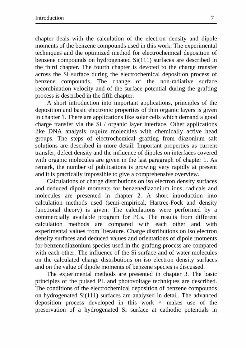
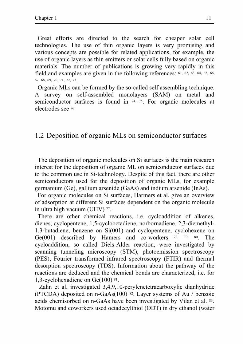
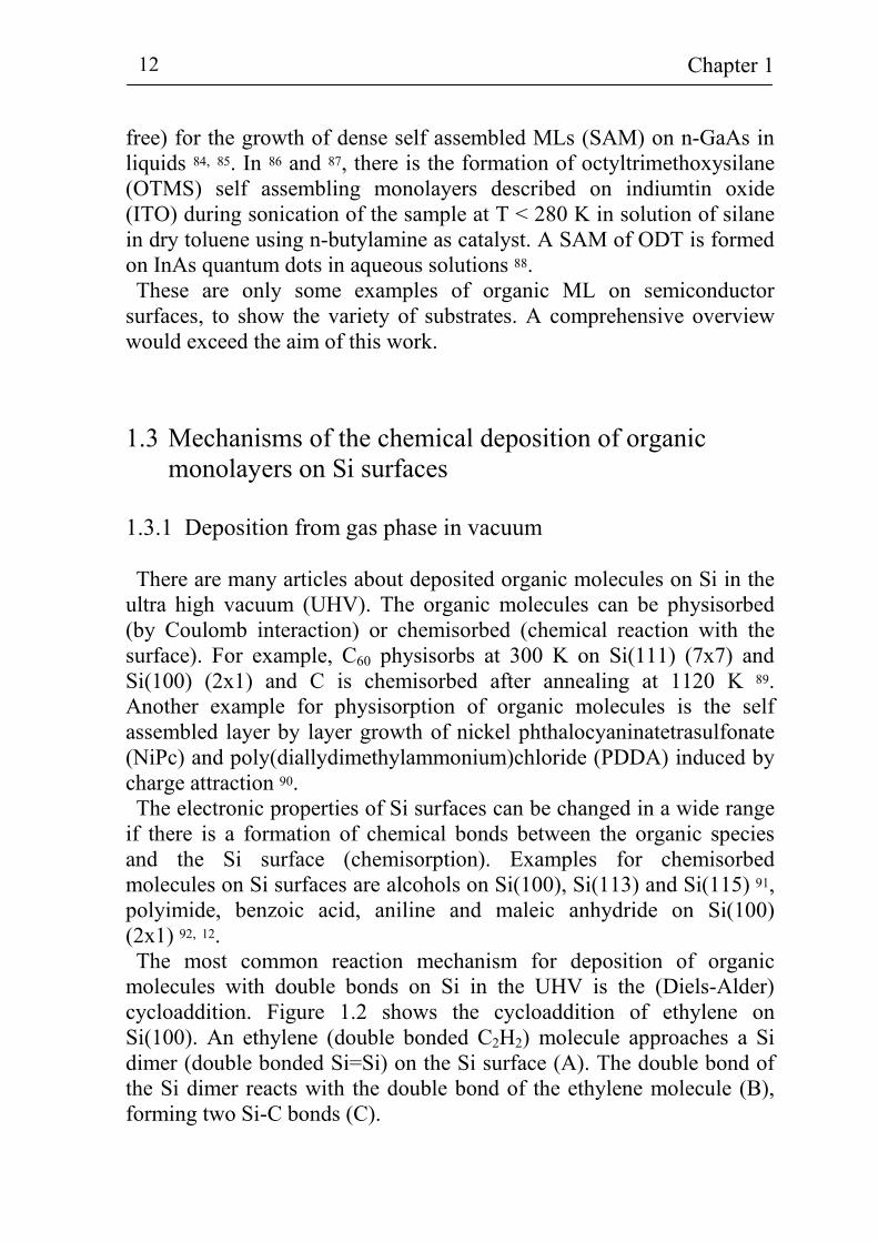
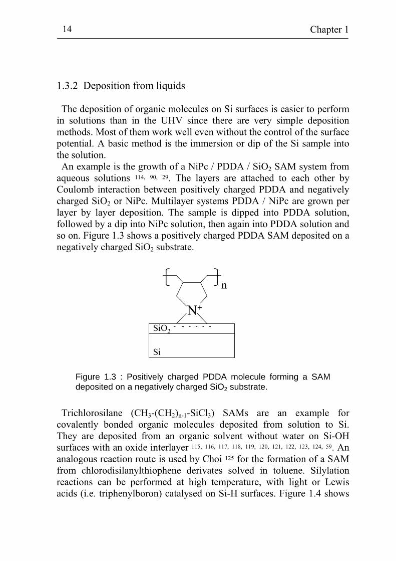
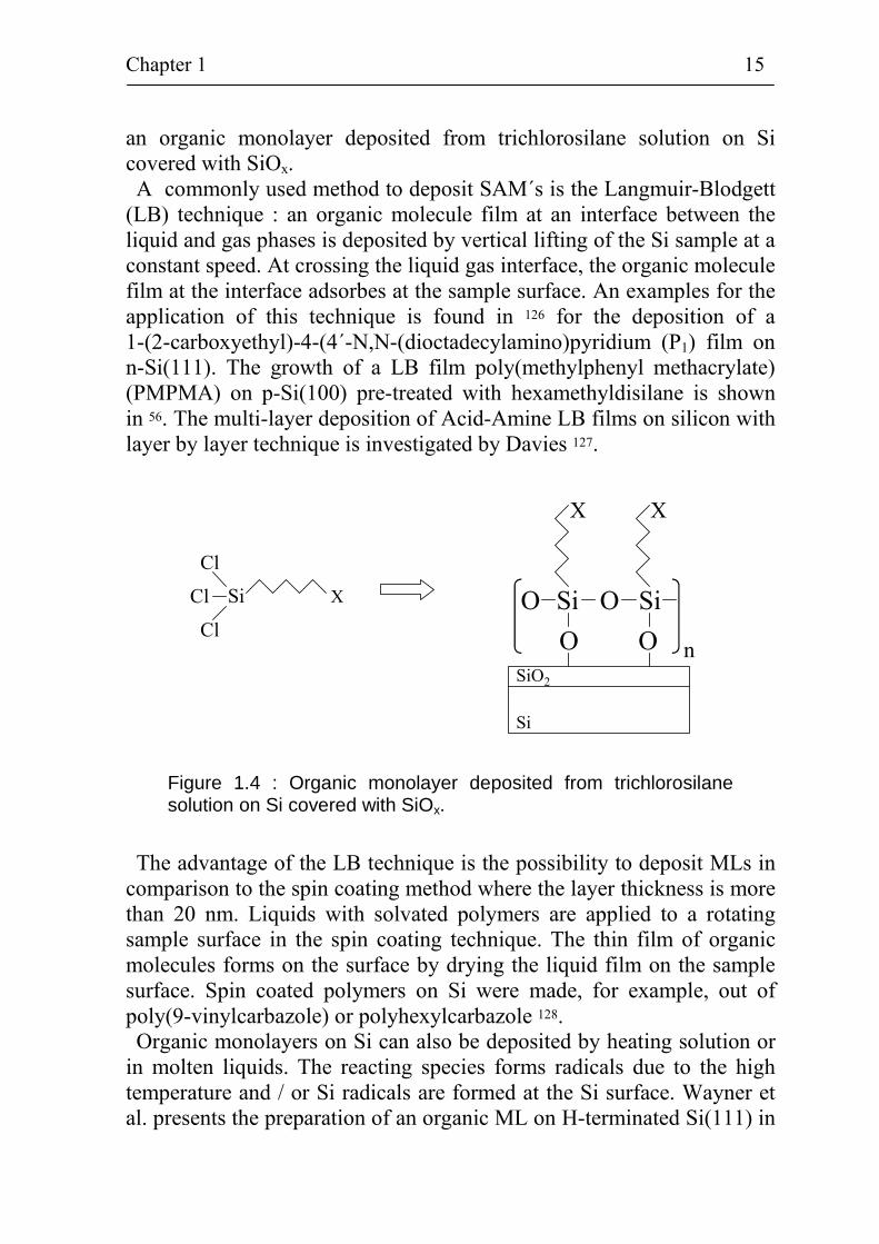
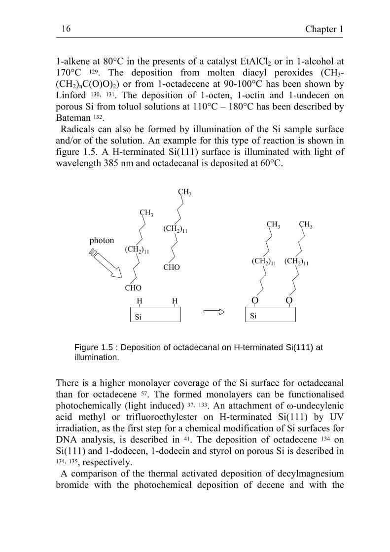
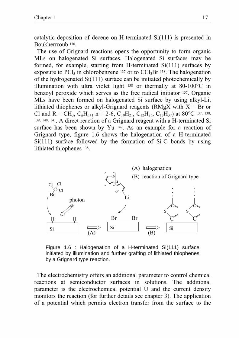
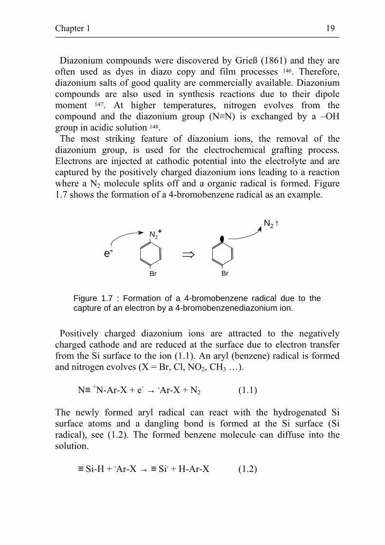
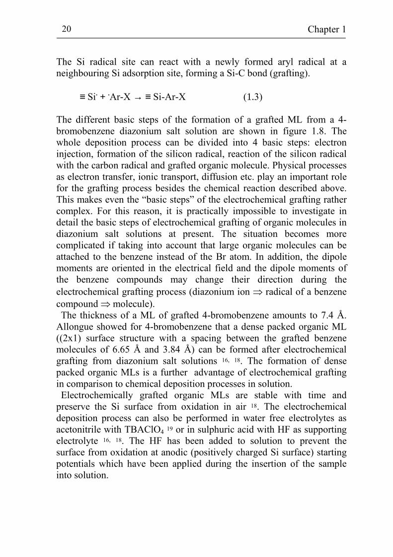
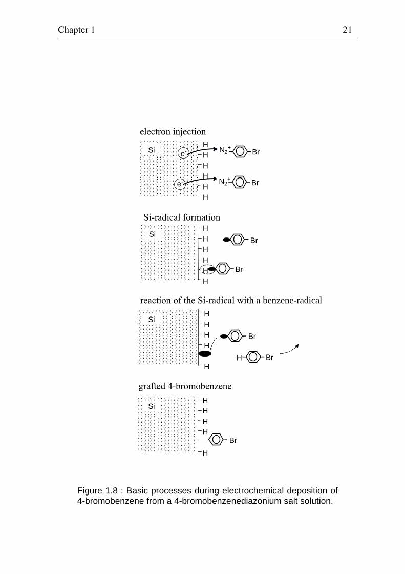
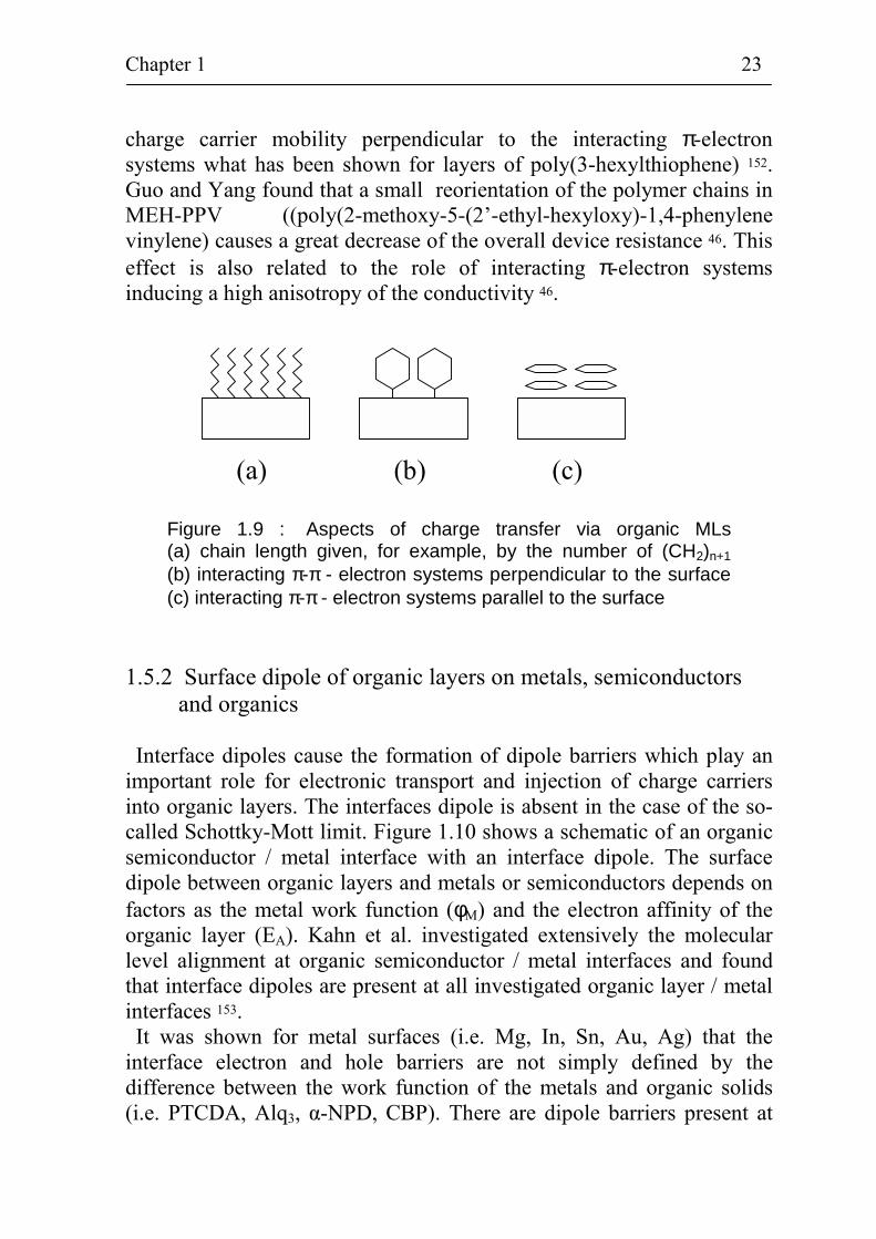
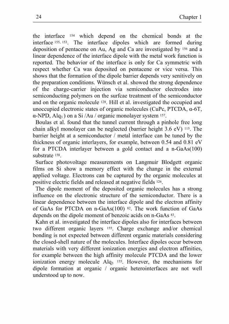

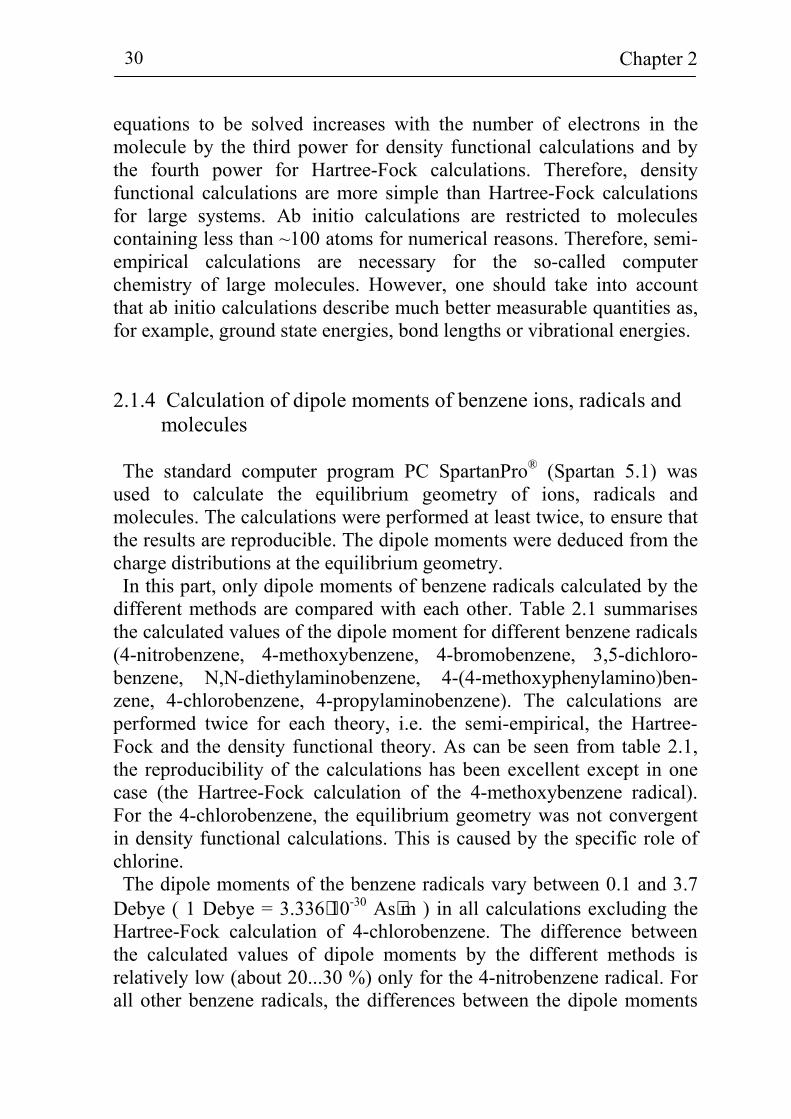
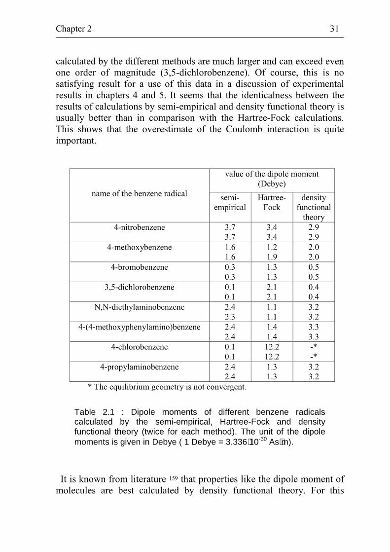
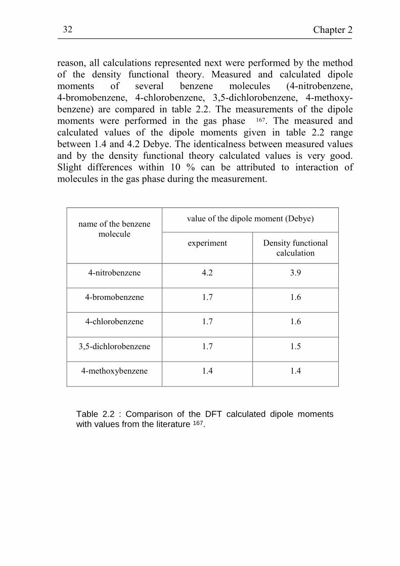
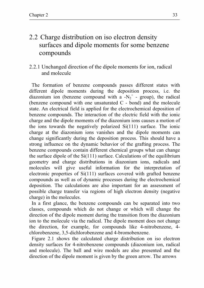
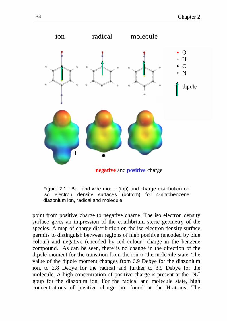
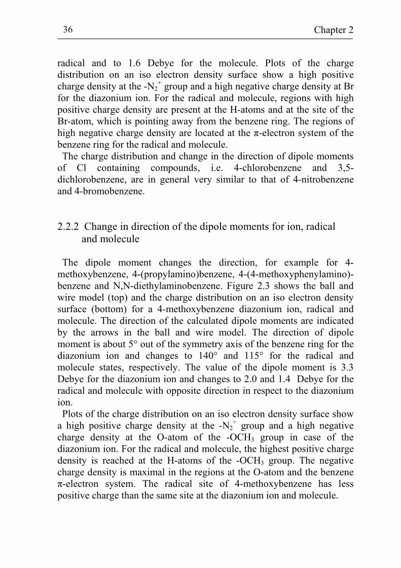
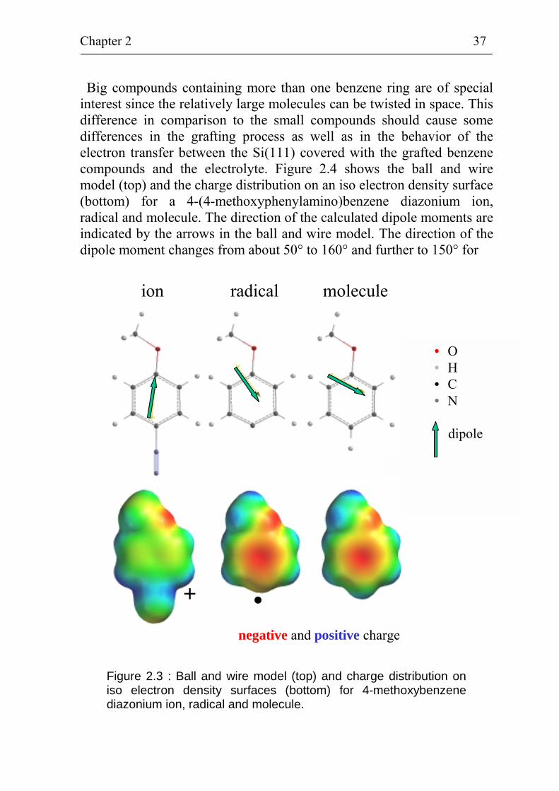
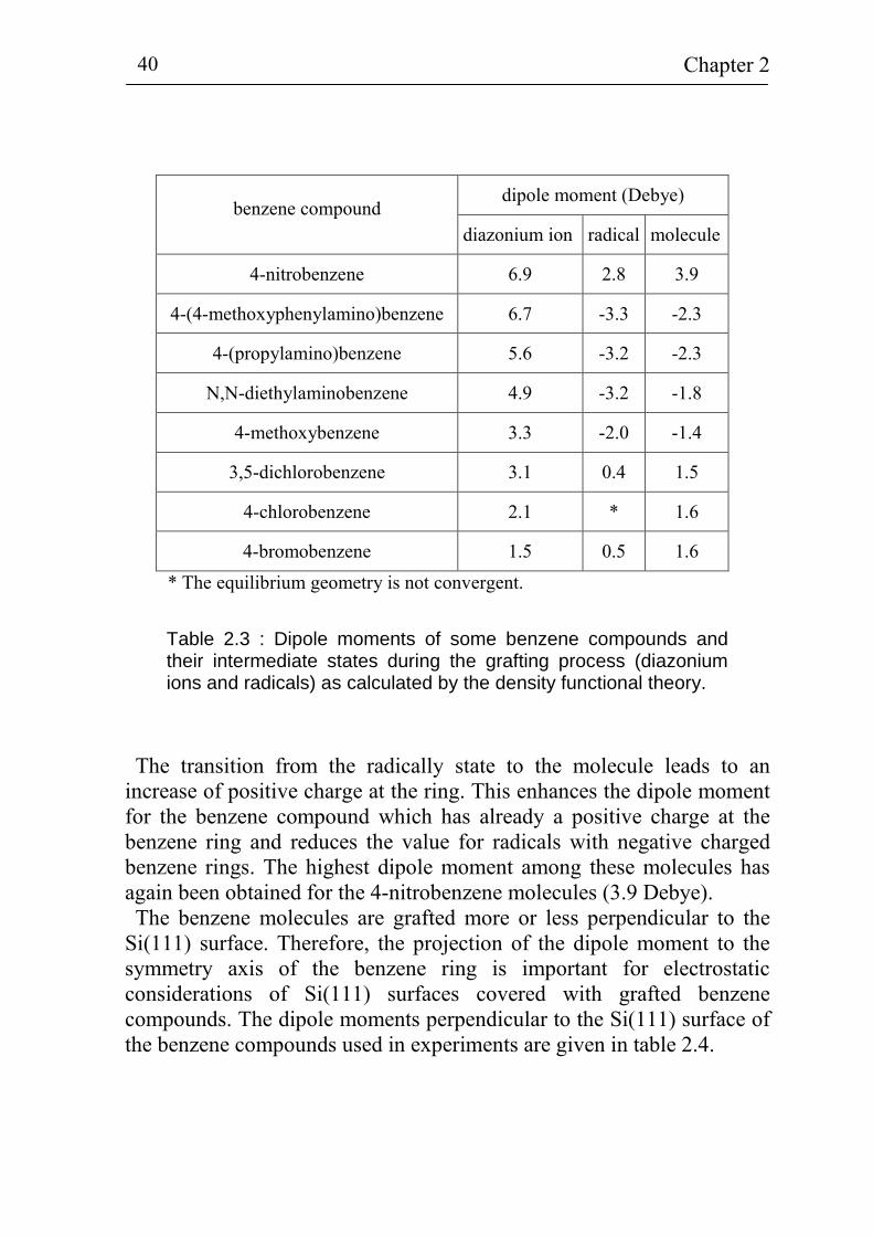
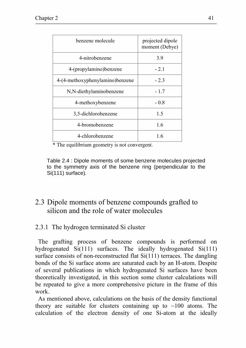
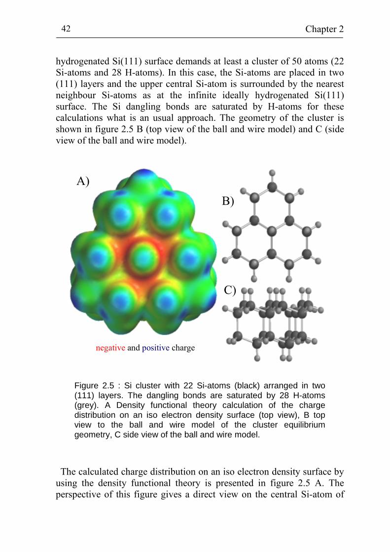
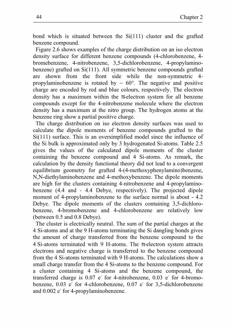
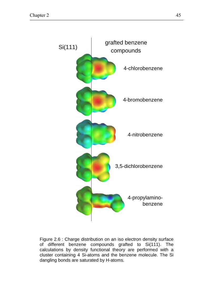
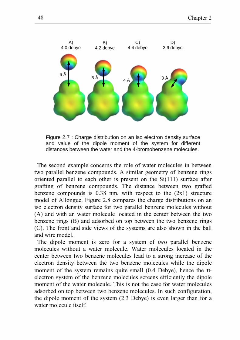
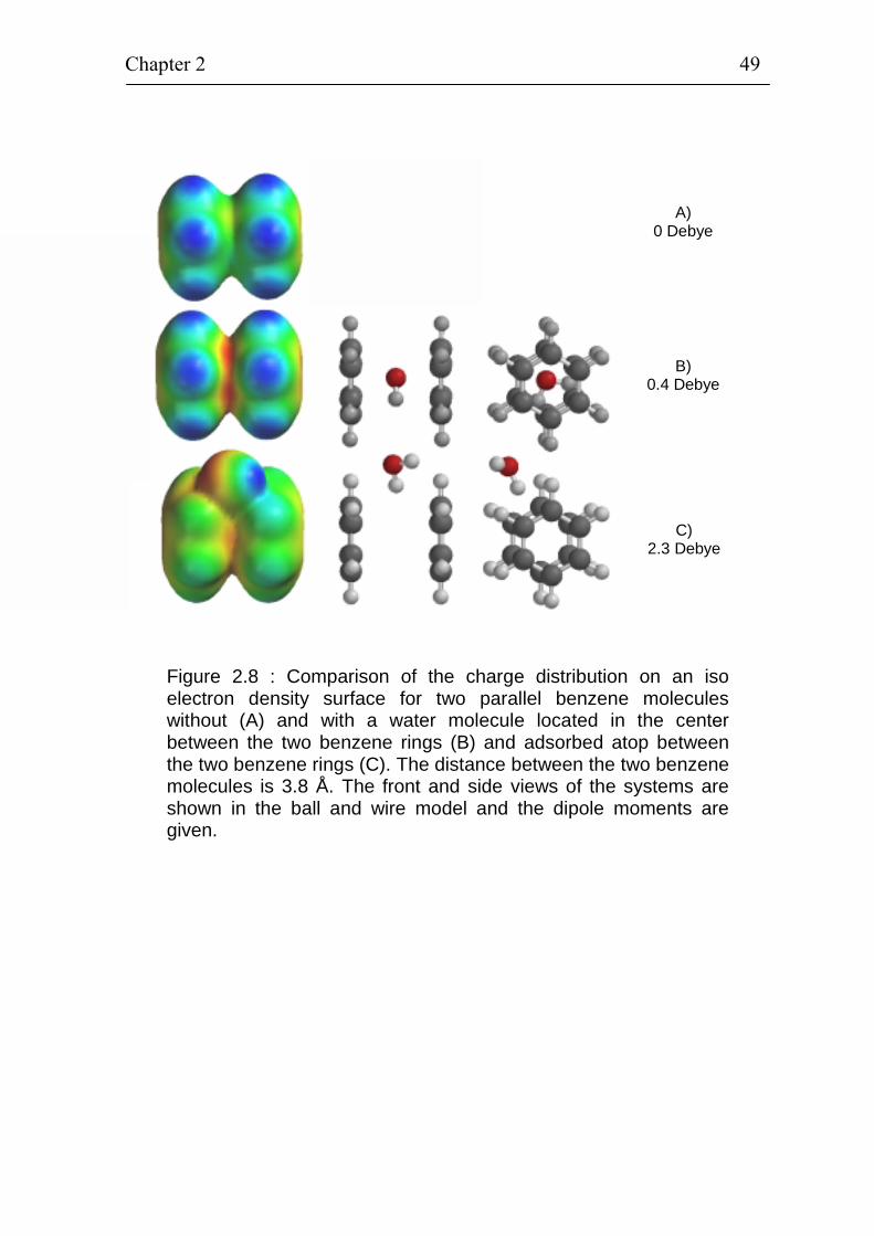
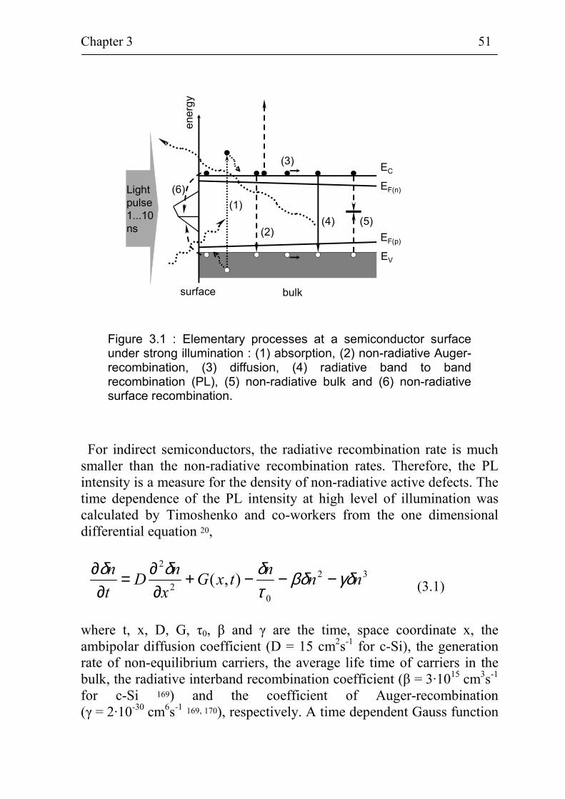
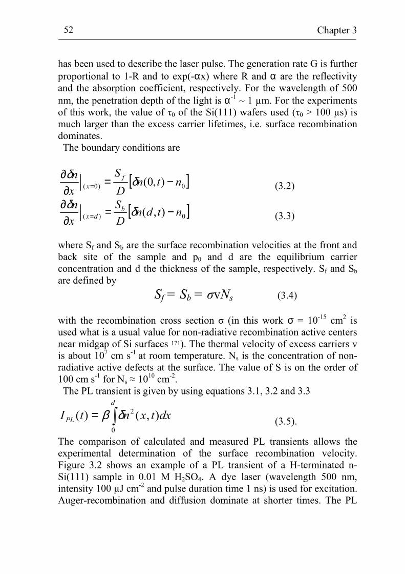
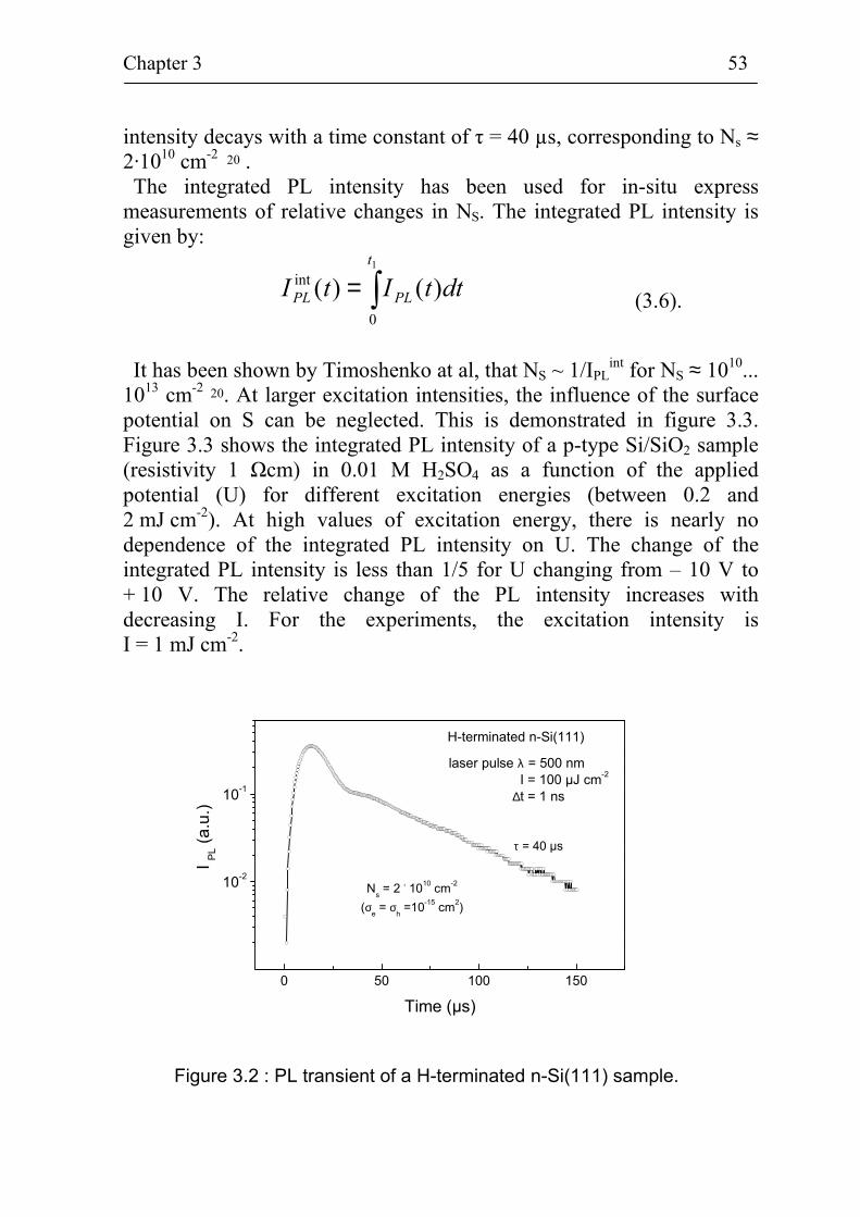
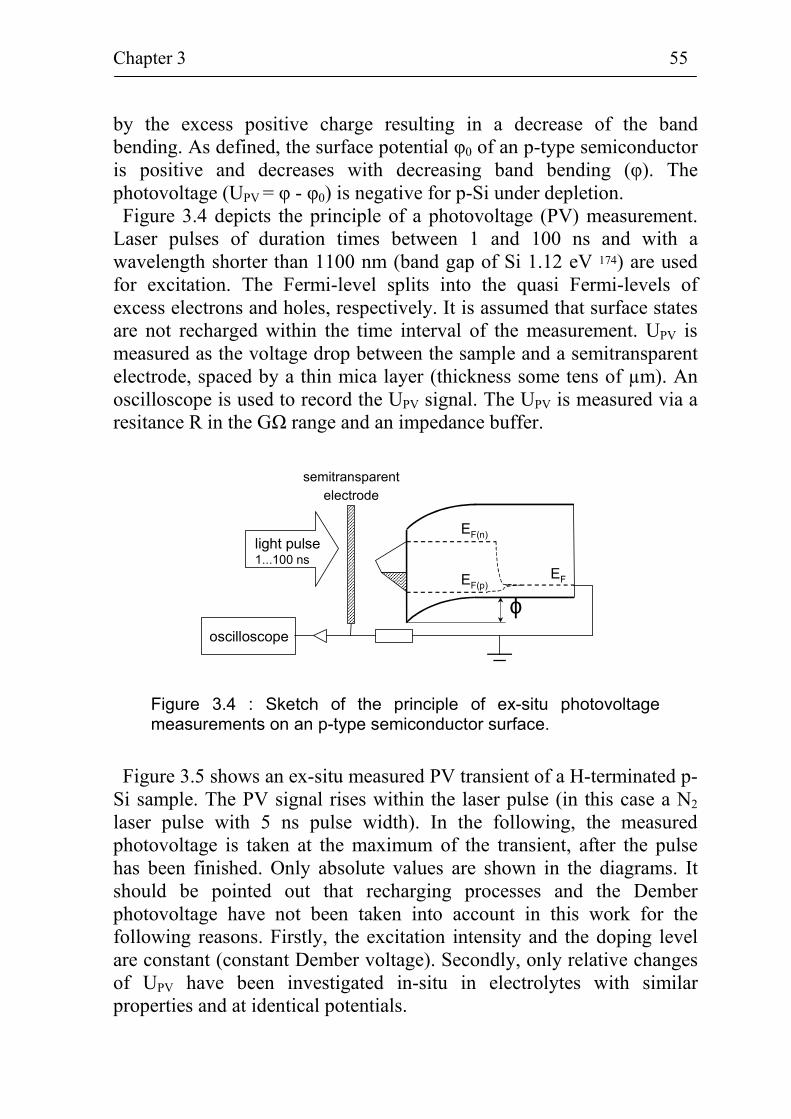
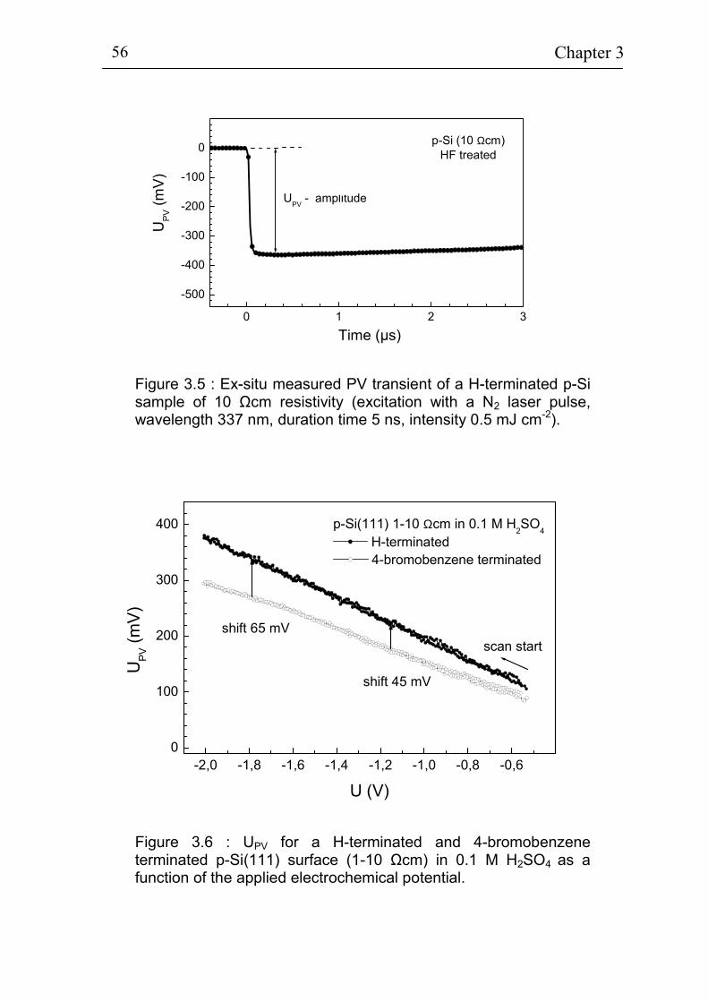
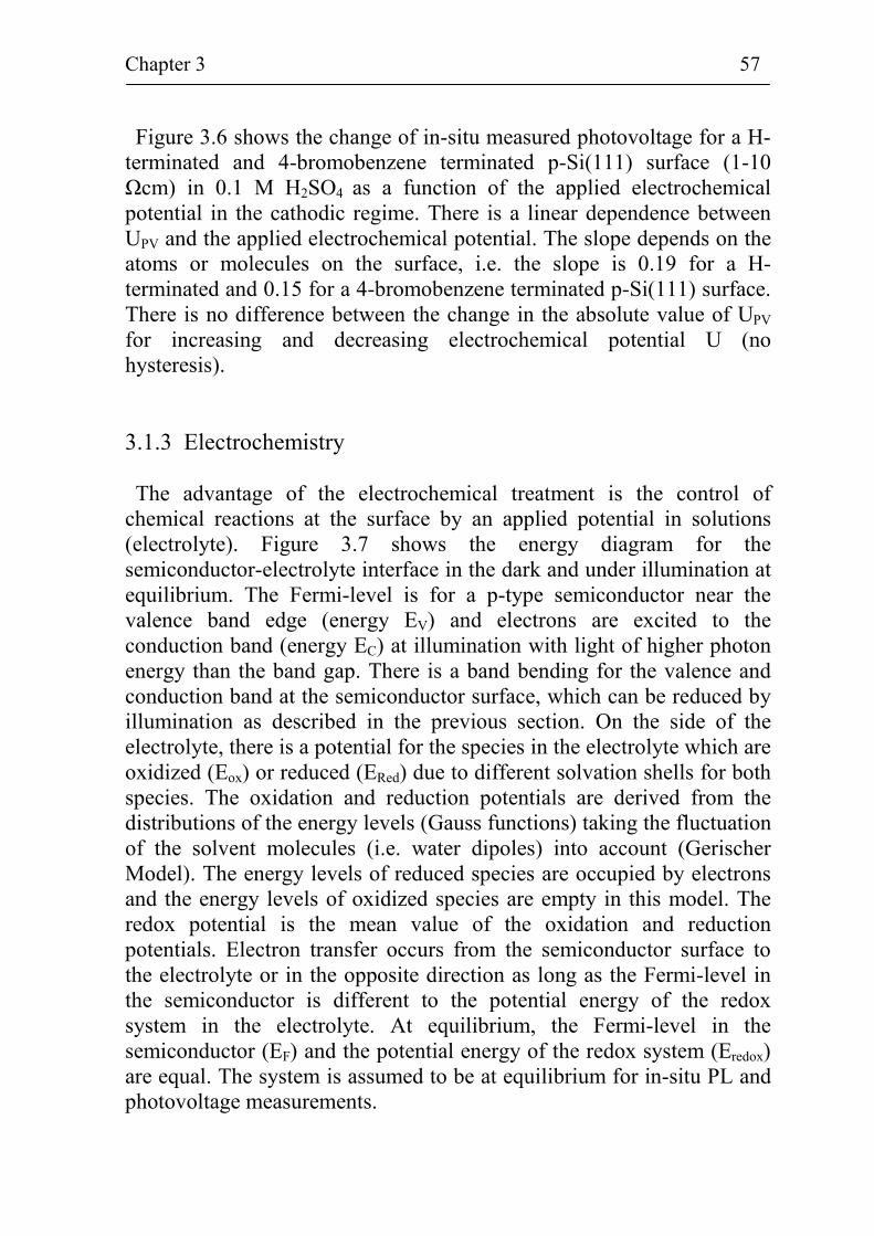
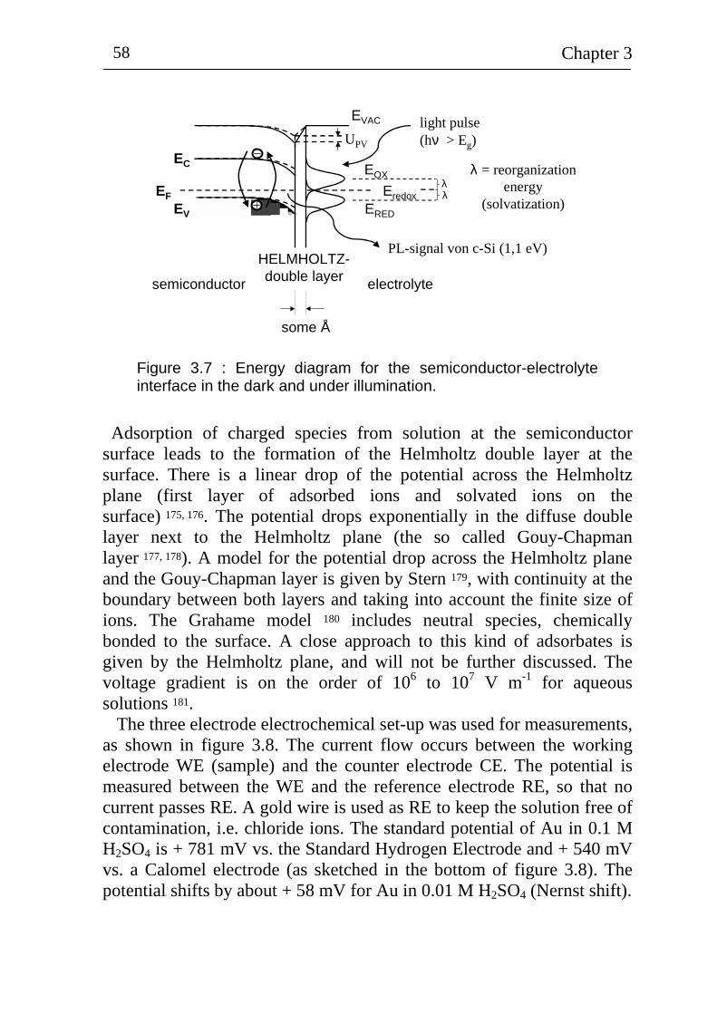
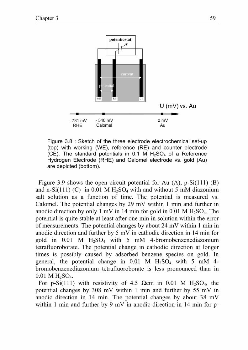
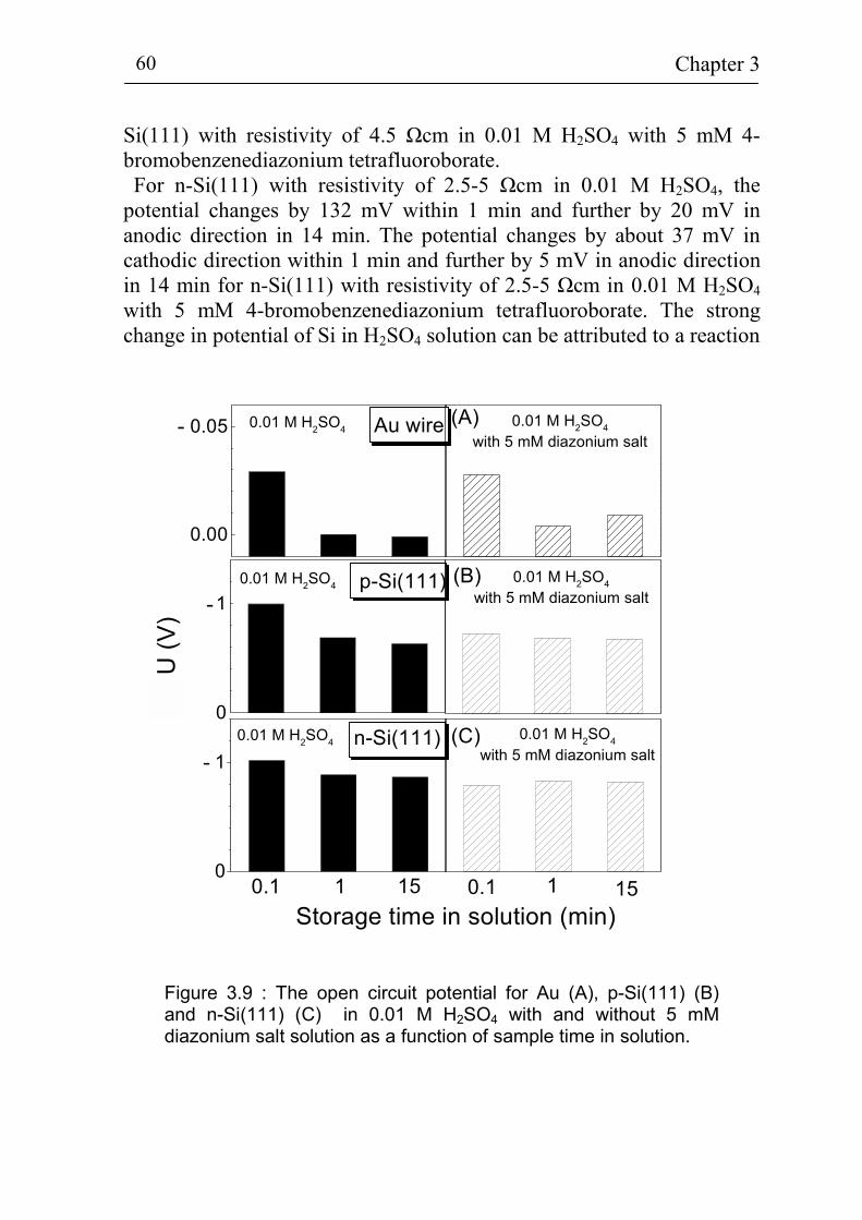
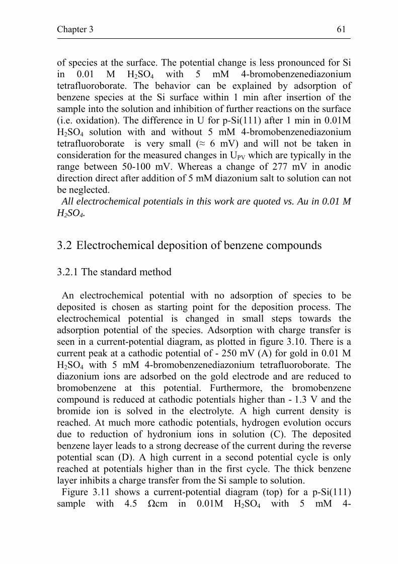
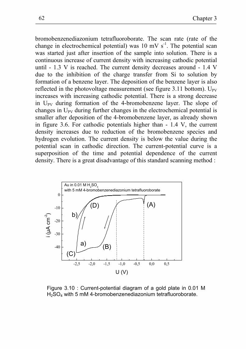
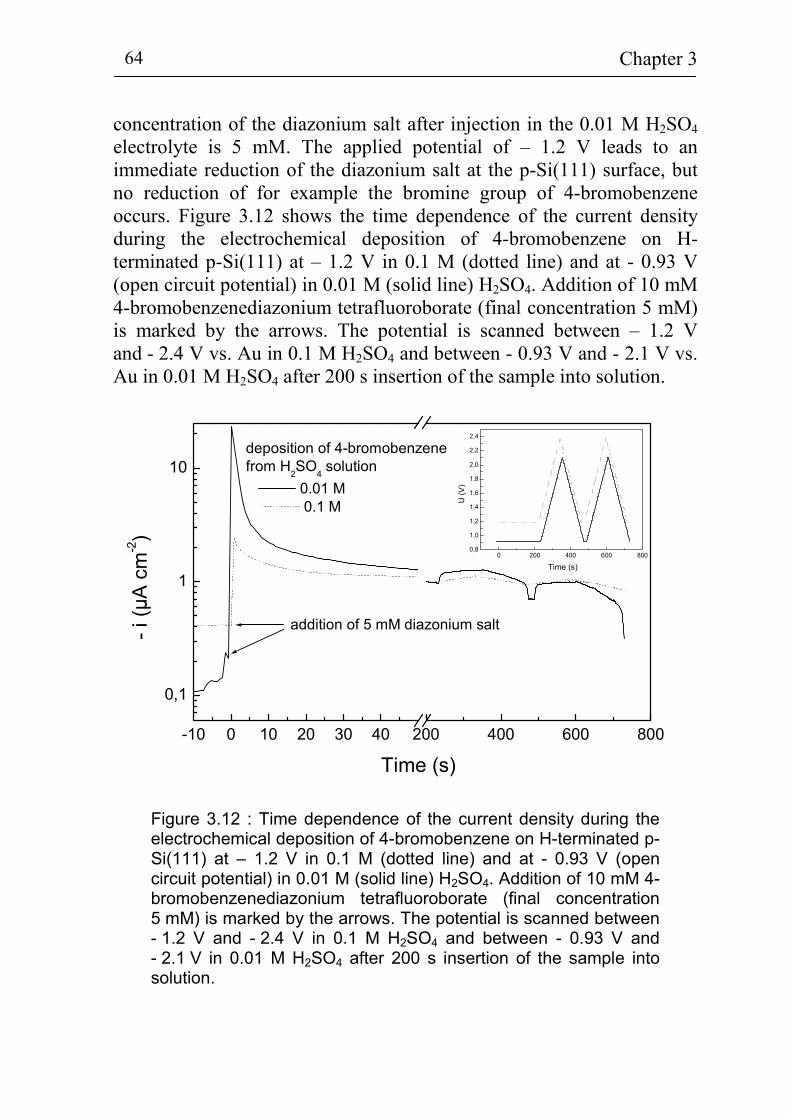
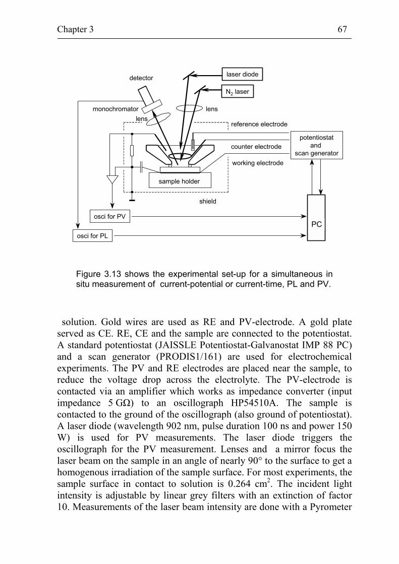

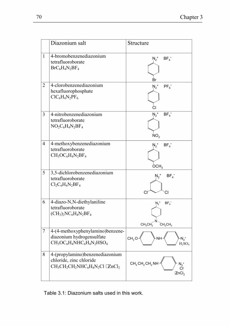
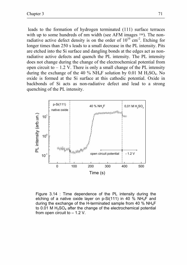
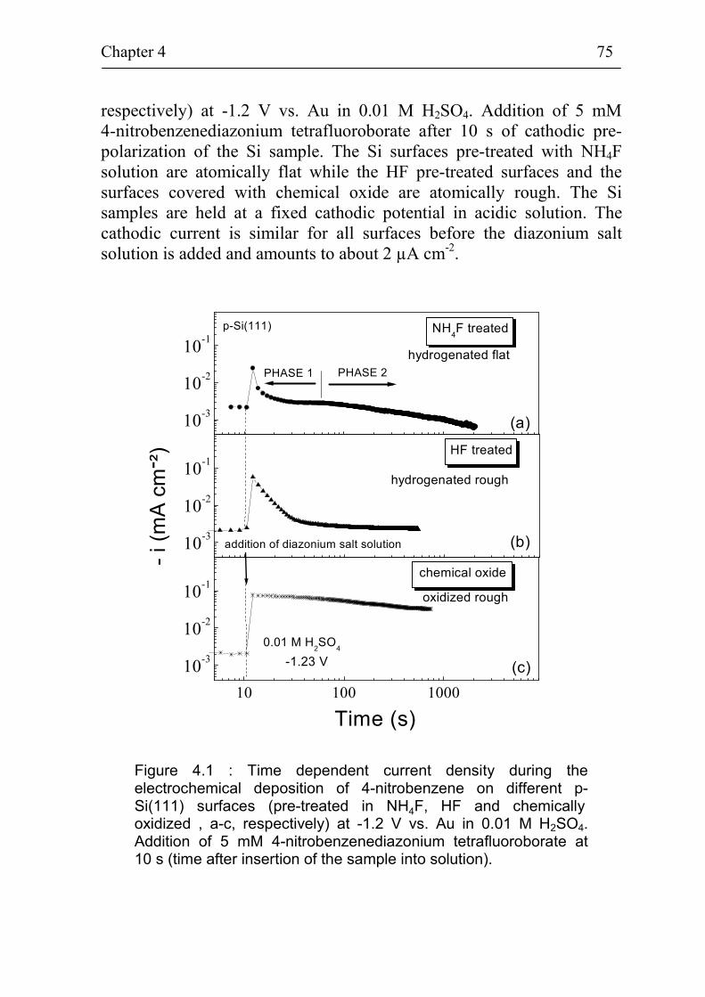
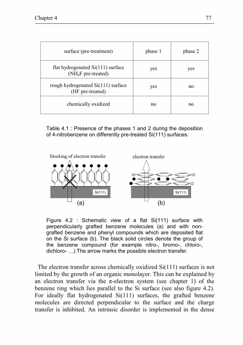
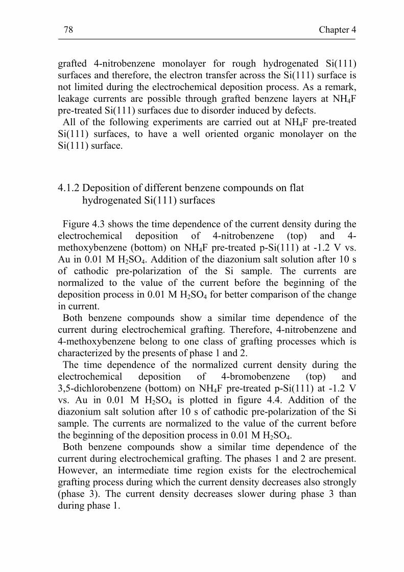
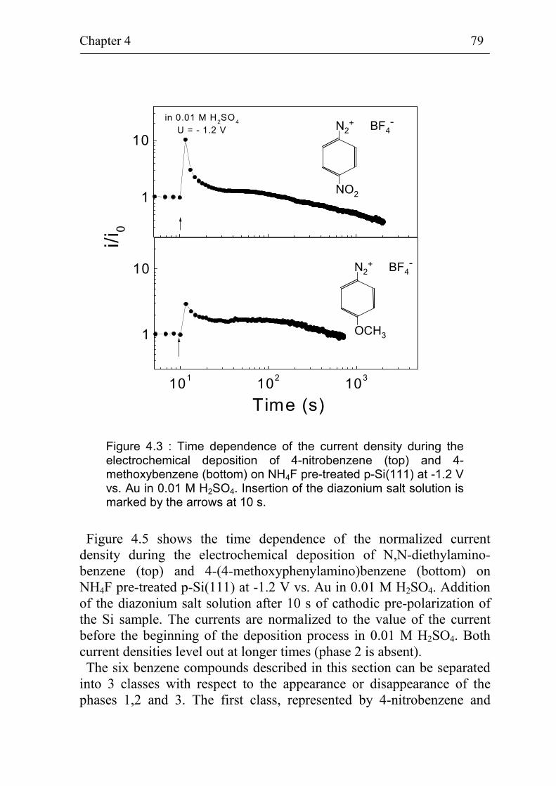
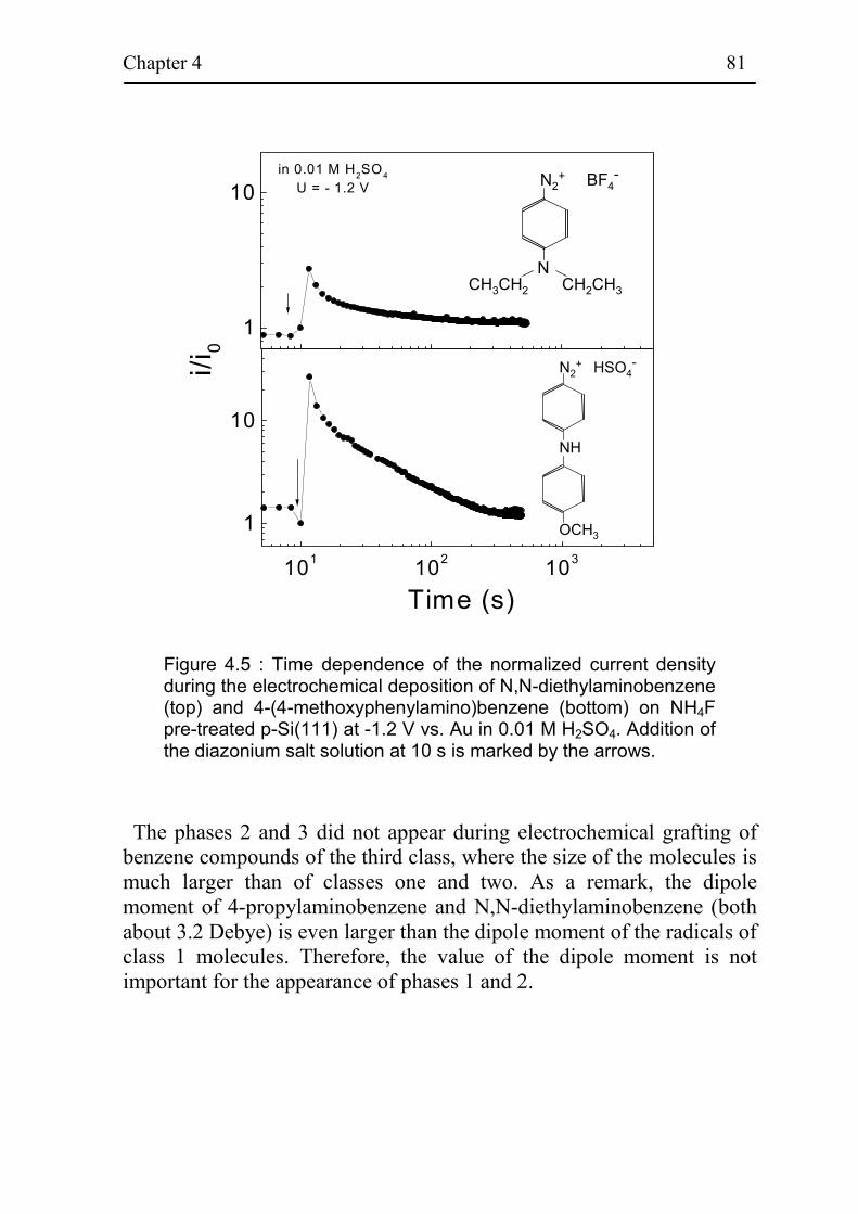
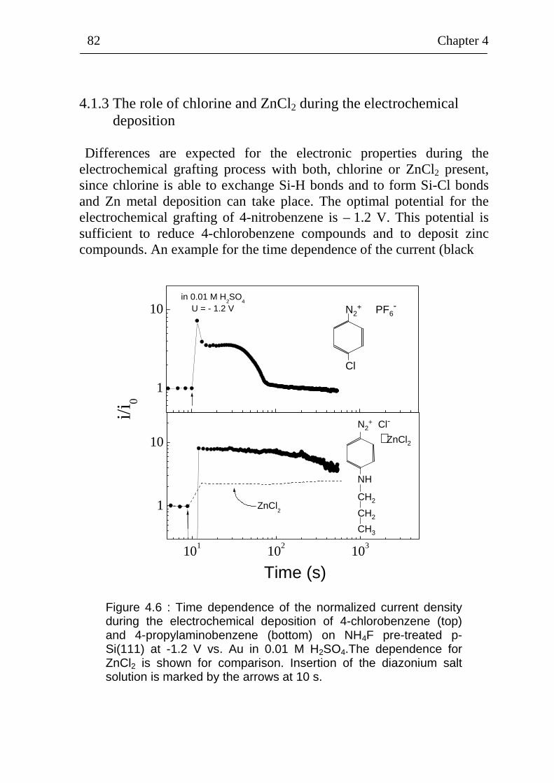
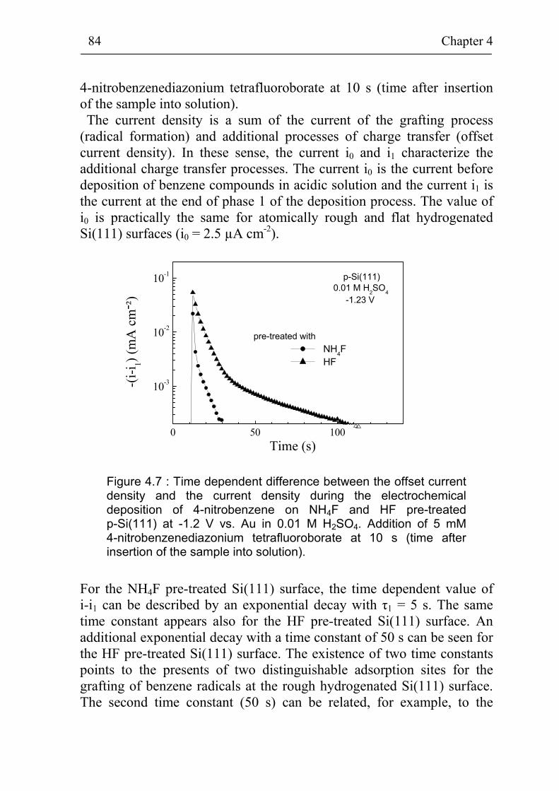
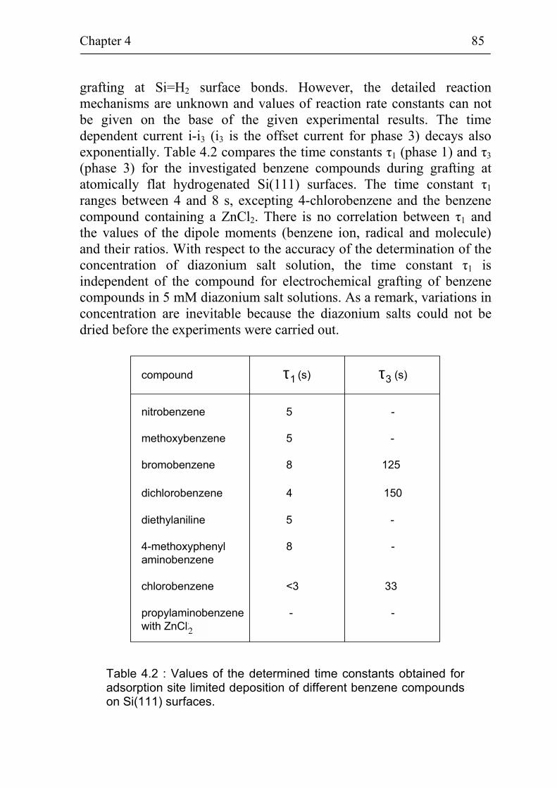
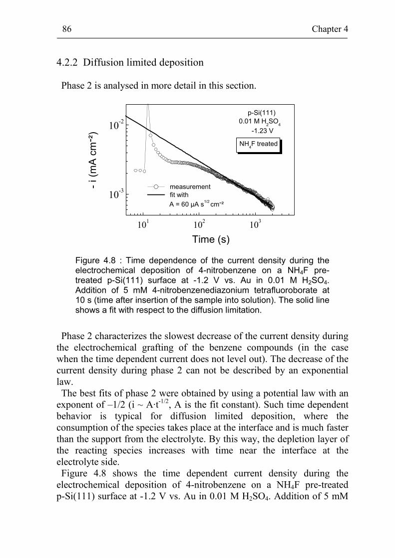
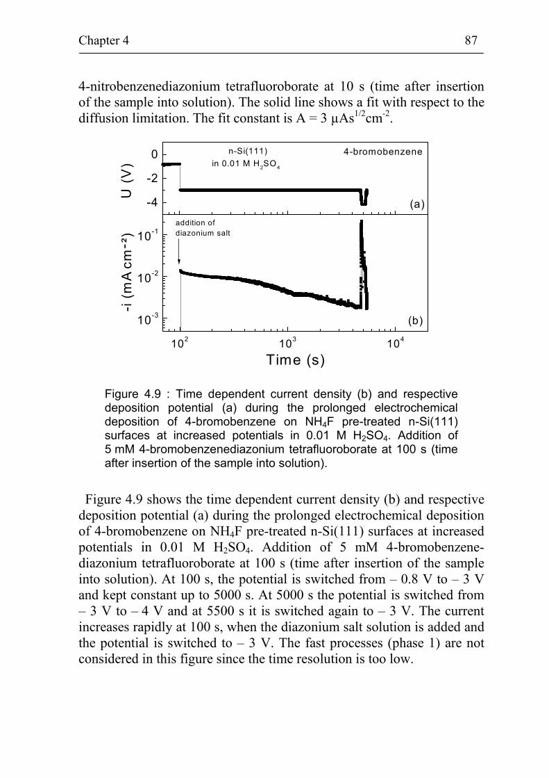
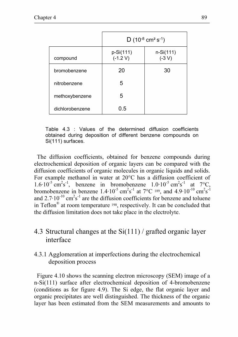
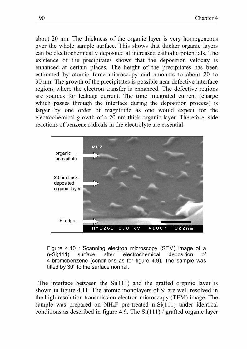
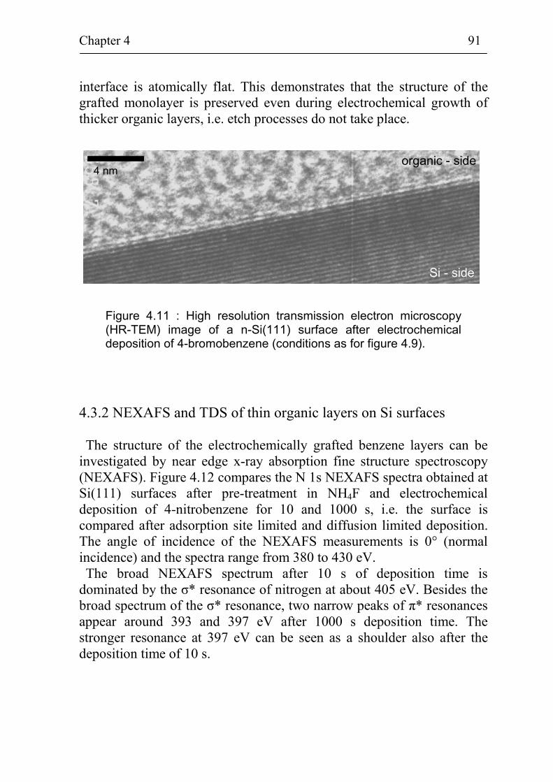
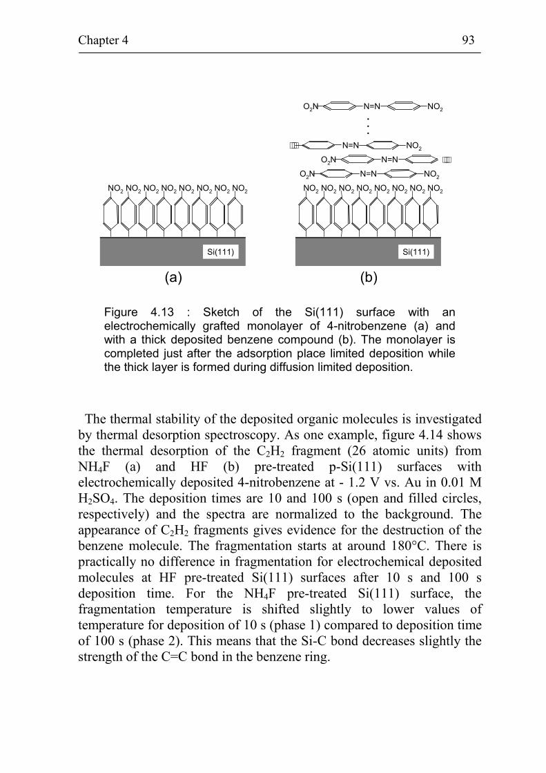
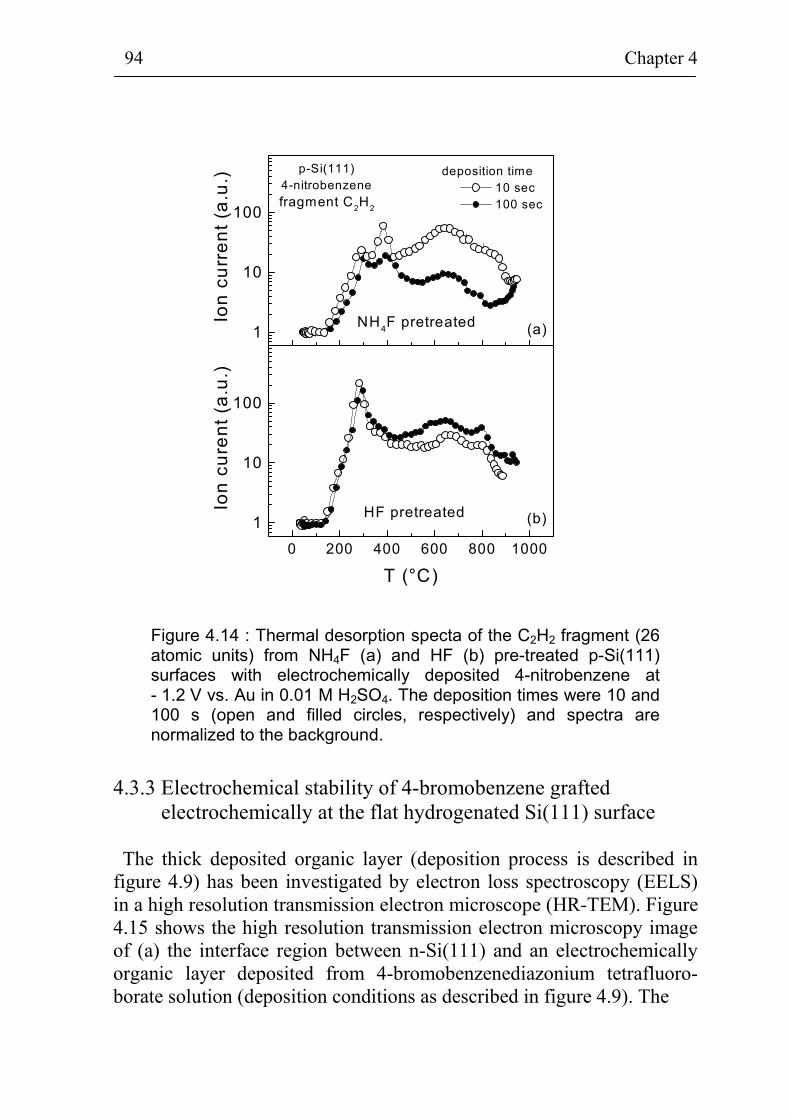
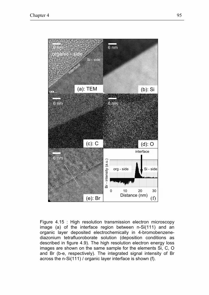
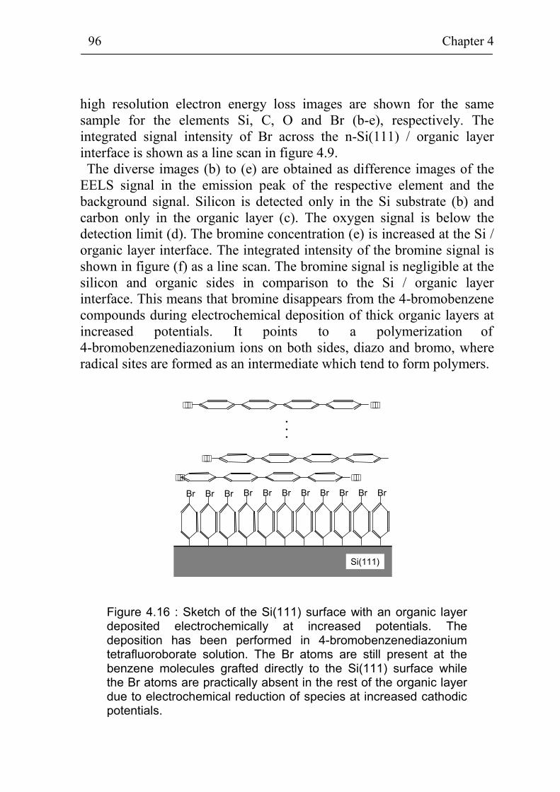
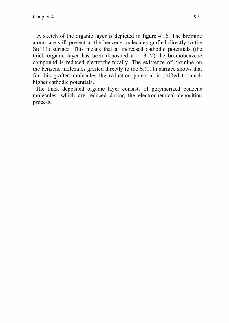
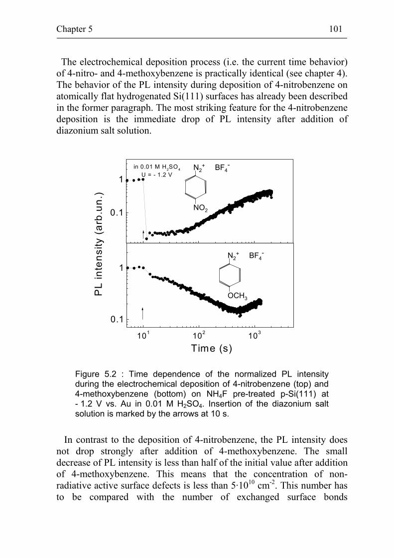
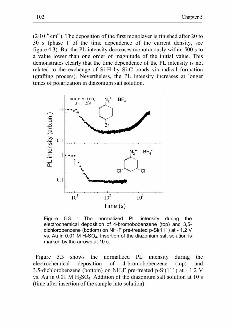
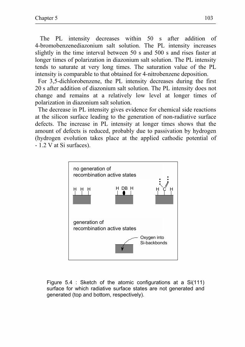
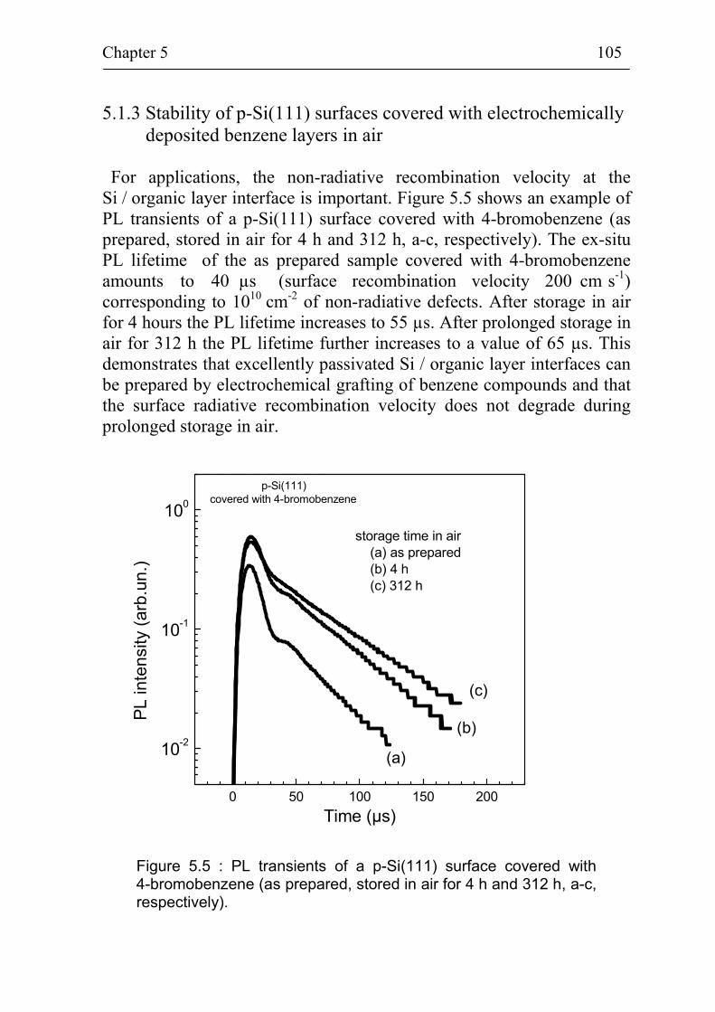
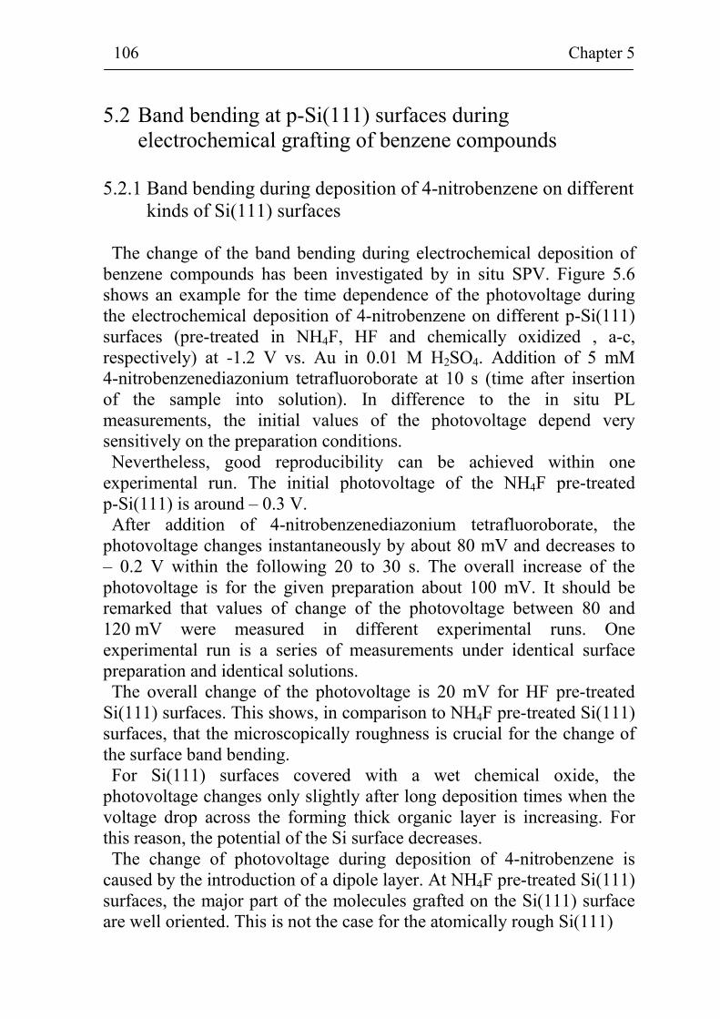
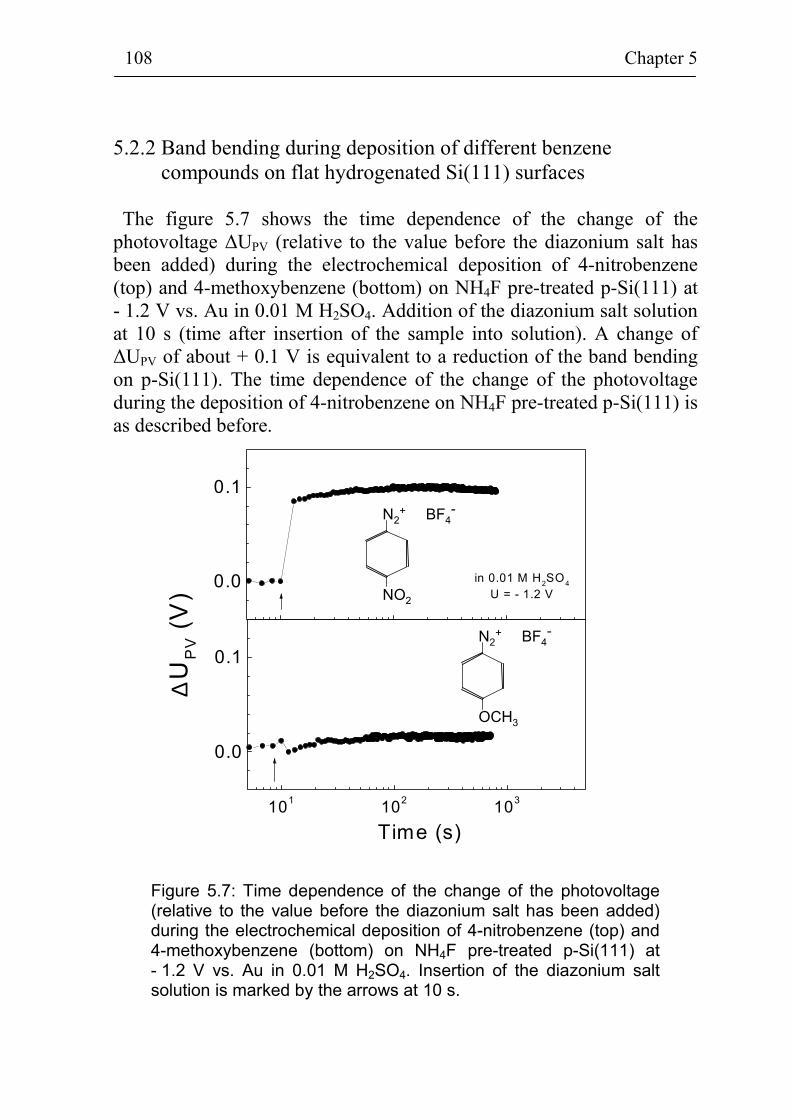
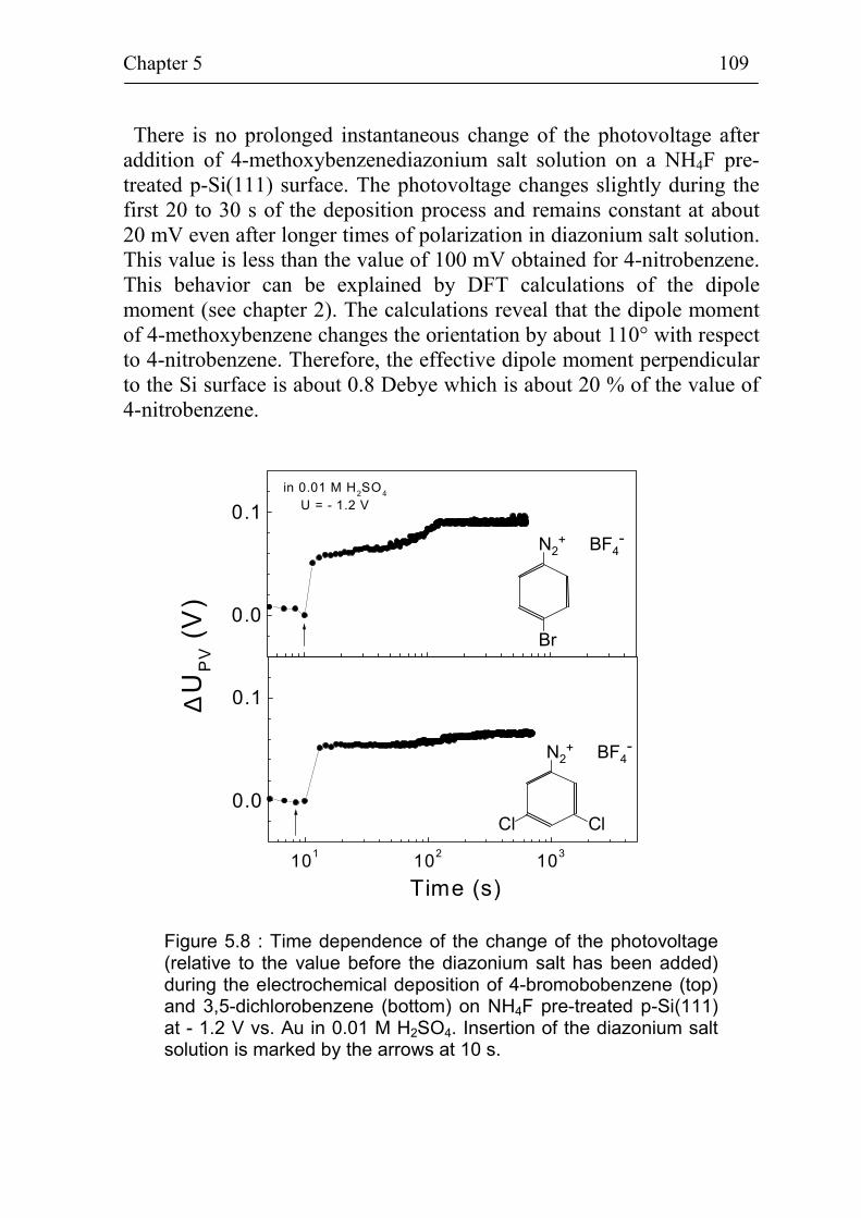
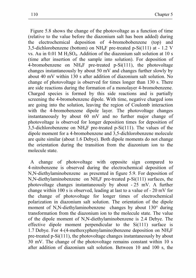
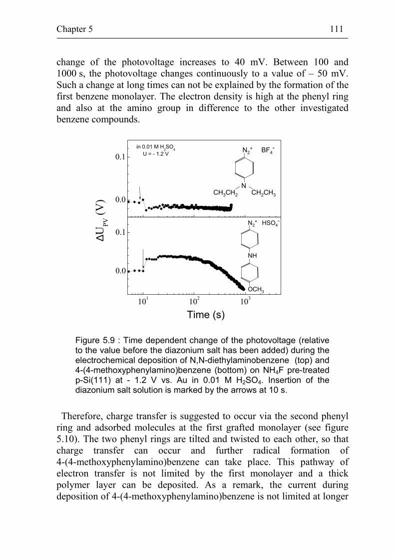
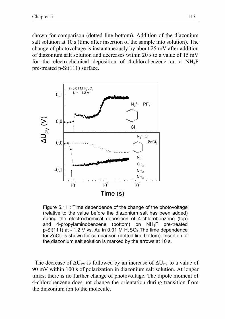
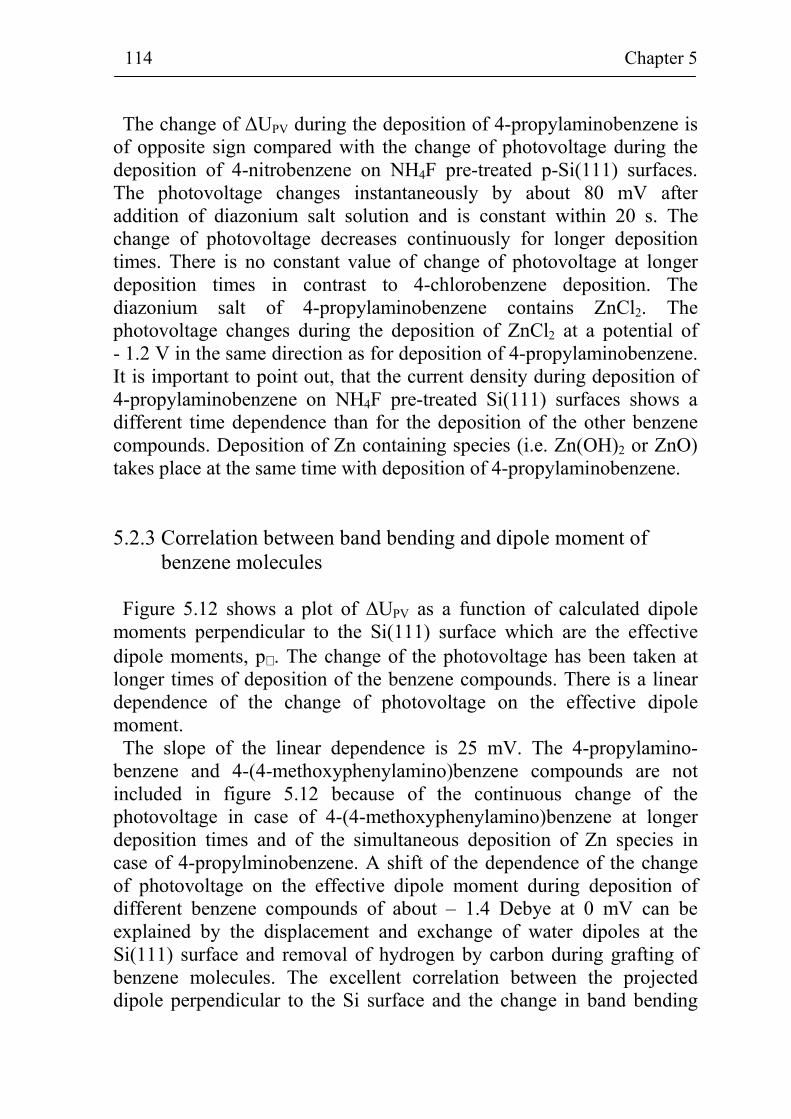
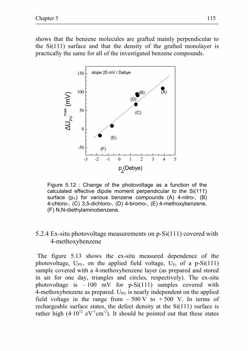
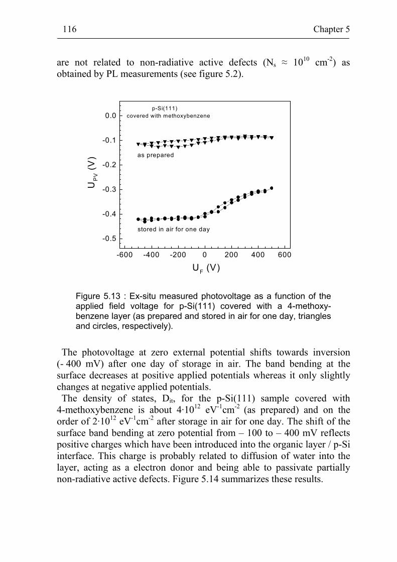
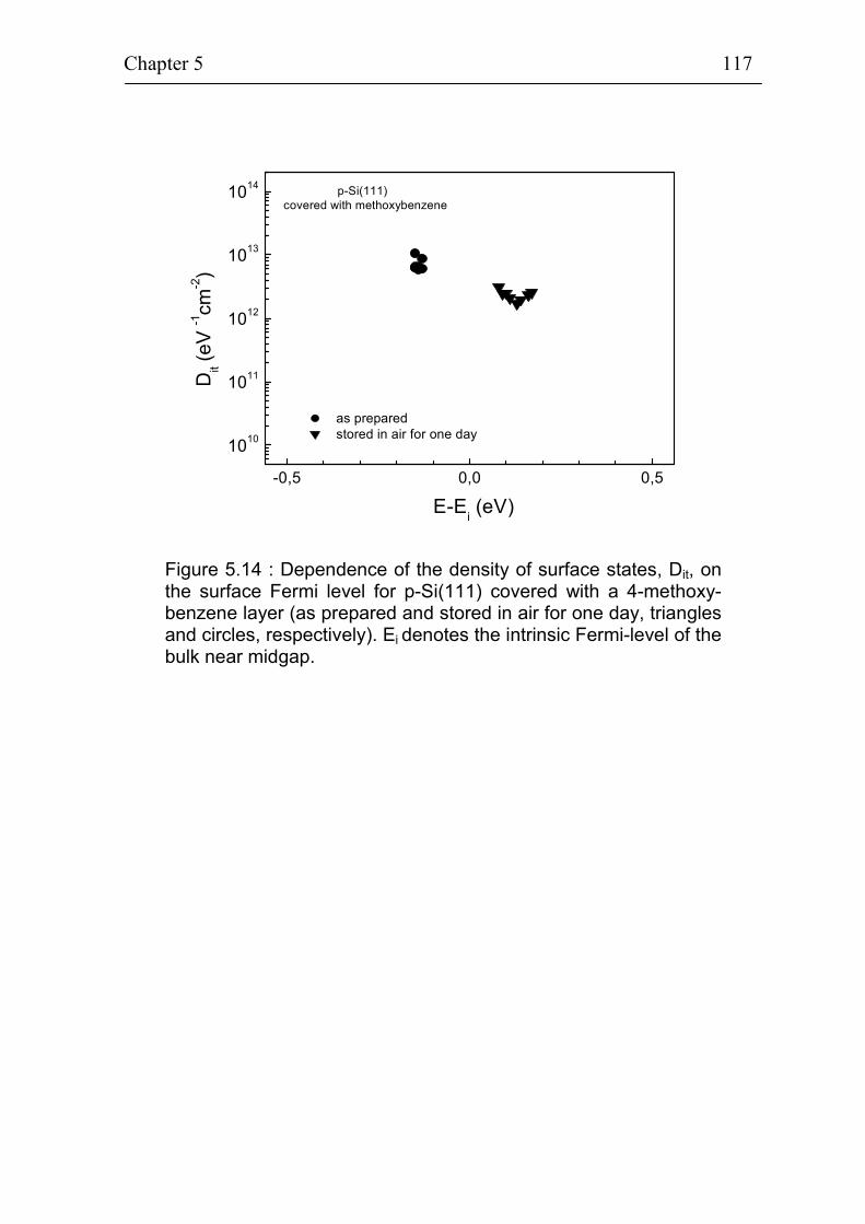
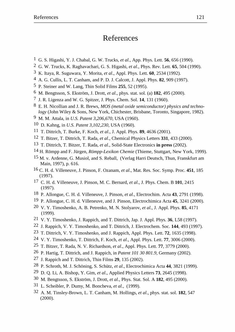
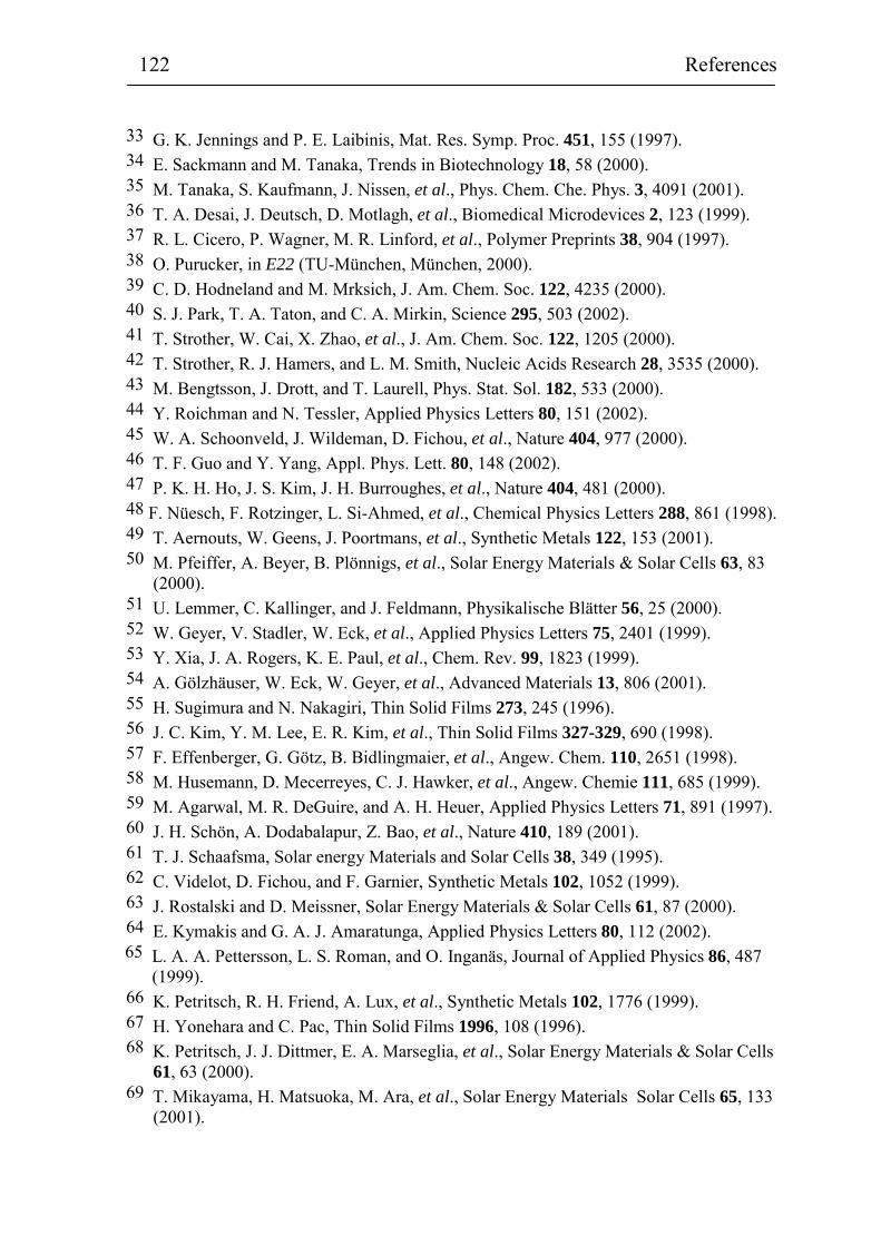
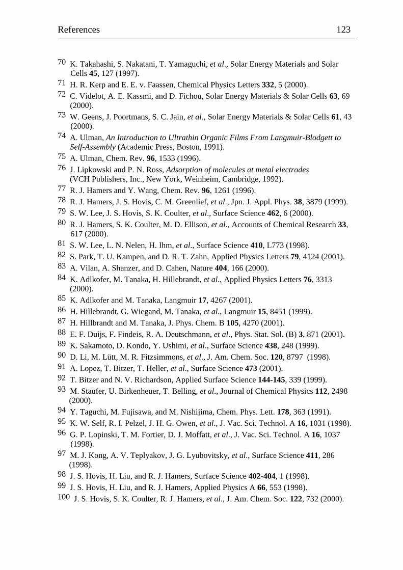
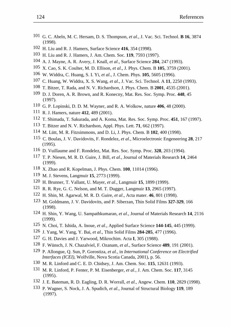


![Automorphisms of Enriques Surfaces · The systematic classification of these surfaces over the complex numbers was then carried out by V. Nikulin [Nik84] and S. Kondo [Kon86]. There](https://static.unterlagen.site/doc/80x56/5fc59b77c932c1371b7a8e41/automorphisms-of-enriques-surfaces-the-systematic-classiication-of-these-surfaces.jpg)


![QM08 002894%20QM08 DE gorchs[1] 271 271 s 272 273 274 279 280 284 285 286 287 337 339 341 344 345 352 353 354 355 356 357 362 363 364 365 111 111 111 111 111 111 111 111 111 111 111](https://static.unterlagen.site/doc/80x56/5d3cfbf688c9938d248b578c/qm08-00289420qm08-de-gorchs1-271-271-s-272-273-274-279-280-284-285-286-287-337.jpg)


