74
DIO4804 Users Manual fi Real Time Devices, Inc. Accessing the Analog World ® Publication No. 4804-9518
DIO4804User�s Manual
®
Real Time Devices, Inc.�Accessing the Analog World�
®
Publication No. 4804-9518

DIO4804User�s Manual
®
REAL TIME DEVICES, INC.Post Office Box 906
State College, Pennsylvania 16804 USAPhone: (814) 234-8087
FAX: (814) 234-5218

Published byReal Time Devices, Inc.
P.O. Box 906State College, PA 16804 USA
Copyright © 1995 by Real Time Devices, Inc.All rights reserved
Printed in U.S.A.
9518
Table of Contents
i
INTRODUCTION .................................................................................................................................... i-1
Digital I/O ............................................................................................................................................................... i-38254 Timer/Counters .............................................................................................................................................. i-3What Comes With Your Board ............................................................................................................................... i-3Board Accessories ................................................................................................................................................... i-3
Hardware Accessories ......................................................................................................................................... i-3Using This Manual .................................................................................................................................................. i-3When You Need Help ............................................................................................................................................. i-4
CHAPTER 1 � BOARD SETTINGS .................................................................................................. 1-1
Factory-Configured Switch and Jumper Settings .................................................................................................. 1-3P19 � 8254 Clock and Gate Source Select (Factory Settings: See Figure 1-2) .............................................. 1-5P20 through P22 � Strobe Input Enable (Factory Setting: Disabled) .............................................................. 1-6S1 � Base Address (Factory Setting: 300 hex (768 decimal)) ......................................................................... 1-7
P7 through P12, Pull-up/Pull-down Resistors on Digital I/O Lines ...................................................................... 1-8
CHAPTER 2 � BOARD INSTALLATION ....................................................................................... 2-1
Board Installation ................................................................................................................................................... 2-3External I/O Connections ....................................................................................................................................... 2-3
Connecting the Digital I/O ................................................................................................................................. 2-4Connecting the Timer/Counter I/O .................................................................................................................... 2-4Connecting the External Interrupt ...................................................................................................................... 2-4
Running the 4804DIAG Diagnostics Program ...................................................................................................... 2-4
CHAPTER 3 � HARDWARE DESCRIPTION................................................................................. 3-1
Digital I/O .............................................................................................................................................................. 3-3Timer/Counters ...................................................................................................................................................... 3-3
CHAPTER 4 � I/O MAPPING ............................................................................................................ 4-1
Defining the I/O Map ............................................................................................................................................. 4-3BA + 0: Digital I/O Port 0 (Read/Write) .......................................................................................................... 4-4BA + 1: Digital I/O Port 1 (Read/Write) ........................................................................................................... 4-4BA + 2: Clear IRQ/Program Port 0 Direction/Port 1 Direction/IRQ Source Registers (Read/Write) ............. 4-4BA + 3: Read Digital I/O Status/Program Digital Mode (Read/Write) ............................................................ 4-5BA + 4: Digital I/O Port 2 (Read/Write) .......................................................................................................... 4-6BA + 5: Digital I/O Port 3 (Read/Write) ........................................................................................................... 4-6BA + 6: Clear IRQ/Program Port 2 Direction/Port 3 Direction/IRQ Source Registers (Read/Write) ............. 4-6BA + 7: Read Digital I/O Status/Program Digital Mode (Read/Write) ............................................................ 4-7BA + 8: Digital I/O Port 4 (Read/Write) .......................................................................................................... 4-8BA + 9: Digital I/O Port 5 (Read/Write) ........................................................................................................... 4-8BA + 10: Clear IRQ/Program Port 4 Direction/Port 5 Direction/IRQ Source Registers (Read/Write) ........... 4-8BA + 11: Read Digital I/O Status/Program Digital Mode (Read/Write) .......................................................... 4-9BA + 12: 8254 Timer/Counter 0 (Read/Write) ............................................................................................... 4-10BA + 13: 8254 Timer/Counter 1 (Read/Write) ............................................................................................... 4-10BA + 14: 8254 Timer/Counter 2 (Read/Write) ............................................................................................... 4-10BA + 15: 8254 Timer/Counter Control Word (Write Only) ........................................................................... 4-10BA + 16: Clear IRQ/IRQ Enable (Read/Write) .............................................................................................. 4-10BA + 17: IRQ Status (Read Only) .................................................................................................................. 4-11
ii
BA + 18: Reserved .......................................................................................................................................... 4-11BA + 19: IRQ Channel/Source Select (Read/Write) ...................................................................................... 4-11
Programming the DIO4804 .................................................................................................................................. 4-12Clearing and Setting Bits in a Port ....................................................................................................................... 4-12
CHAPTER 5 � DIGITAL I/O ............................................................................................................. 5-1
Bit Programmable Digital I/O ................................................................................................................................ 5-3Digital Interrupts .................................................................................................................................................... 5-3Resetting the Digital Circuitry ............................................................................................................................... 5-3Strobing Data into Ports 0, 2, and 4 ....................................................................................................................... 5-3
CHAPTER 6 � TIMER/COUNTERS ................................................................................................. 6-1
CHAPTER 7 � INTERRUPTS ............................................................................................................ 7-1
Software Programmable Interrupts ........................................................................................................................ 7-3Digital Interrupts .................................................................................................................................................... 7-3
Sampling Digital Lines for Change of State ...................................................................................................... 7-3Selecting the Interrupt Channel .............................................................................................................................. 7-3Basic Programming For Interrupt Handling .......................................................................................................... 7-4
What Is an Interrupt? ......................................................................................................................................... 7-4Interrupt Request Lines ...................................................................................................................................... 7-48259 Programmable Interrupt Controller .......................................................................................................... 7-4
Interrupt Mask Register (IMR) ...................................................................................................................... 7-4End-of-Interrupt (EOI) Command ................................................................................................................. 7-4
What Exactly Happens When an Interrupt Occurs? .......................................................................................... 7-5Using Interrupts in Your Programs .................................................................................................................... 7-5Writing an Interrupt Service Routine (ISR) ....................................................................................................... 7-5Saving the Startup Interrupt Mask Register (IMR) and Interrupt Vector .......................................................... 7-7Restoring the Startup IMR and Interrupt Vector ............................................................................................... 7-7Common Interrupt Mistakes .............................................................................................................................. 7-7
APPENDIX A � DIO4804 SPECIFICATIONS ................................................................................. A-1
APPENDIX B � CONNECTOR PIN ASSIGNMENTS .................................................................... B-1
APPENDIX C � COMPONENT DATA SHEETS ............................................................................ C-1
APPENDIX D � WARRANTY............................................................................................................ D-1
List of Illustrations
1-1 Board Layout Showing Factory-Configured Settings .............................................................................. 1-41-2 8254 Clock and Gate Sources Jumpers, P19 ............................................................................................ 1-51-3 8254 Circuit Diagram ............................................................................................................................... 1-61-4 Port 0 Strobe Input Enable Jumper, P20 .................................................................................................. 1-61-5 Base Address Switch, S1 .......................................................................................................................... 1-71-6 Port 0 Pull-up/Pull-down Resistor Connections, P7 ................................................................................. 1-82-1 P2, P3, and P6 I/O Connector Pin Assignments ....................................................................................... 2-43-1 DIO4804 Block Diagram ......................................................................................................................... 3-33-2 Timer/Counter Circuit Block Diagram ..................................................................................................... 3-46-1 8254 Timer/Counter Circuit Block Diagram ............................................................................................ 6-37-1 Digital Interrupt Timing Diagram ............................................................................................................ 7-3
iii

iv

i-1
INTRODUCTION

i-2
i-3
The DIO4804 opto-22 compatible digital I/O Advanced Industrial Control board is for use in an IBM PC-compatible computer. Installed in a single full-size slot, the DIO4804 features:
� 48 bit programmable digital I/O lines,� Pull-up/pull-down resistors on each bit,� Three 16-bit timer/counters and on-board 8 MHz clock,� Direct connection to opto-22 I/O system modules,� Operation from single +5V supply,� DOS example programs with source code in QuickBASIC and C,� Diagnostics software.
The following paragraphs briefly describe the major functions of the board. A detailed discussion of boardfunctions is included in subsequent chapters.
Digital I/O
The DIO4804 has 48 bit-programmable buffered TTL/CMOS digital I/O lines which are grouped into six 8-bitports, Port 0 through Port 5. Three custom digital ICs handle the digital I/O circuitry, with each IC containing twoports, or 16 bit programmable digital I/O lines.
Bit configurable pull-up or pull-down resistors are provided for all 48 lines. Instructions for activating thesepull-up/pull-down resistors are given at the end of Chapter 1, Board Settings.
8254 Timer/Counters
An 8254 programmable interval timer provides three 16-bit, 8 MHz timer/counters to support a wide range ofuser timing and counting functions.
What Comes With Your Board
You receive the following items in your board package:
� DIO4804 opto-22 compatible digital control board� DOS example programs in QuickBASIC and C with source code & diagnostics software� User�s manual
If any item is missing or damaged, please call Real Time Devices� Customer Service Department at(814) 234-8087. If you require service outside the U.S., contact your local distributor.
Board Accessories
In addition to the items included in your board package, Real Time Devices offers a full line of software andhardware accessories. Call your local distributor or our main office for more information about these accessories andfor help in choosing the best items to support your board�s application.
Hardware Accessories
Hardware accessories for the DIO4804 include the DOP series optoisolated digital input front-end boards, theDMR series mechanical relay output front-end boards, the TB50 terminal board and XB50 prototype/terminal boardfor easy signal access and prototype development, and XO50 ribbon cable assembly for interconnection to anopto-22 rack.
Using This Manual
This manual is intended to help you install your new board and get it running quickly, while also providingenough detail about the board and its functions so that you can enjoy maximum use of its features even in the mostcomplex applications. We assume that you already have an understanding of data acquisition principles and that youcan customize the example software or write your own application programs.

i-4
When You Need Help
This manual and the example programs in the software package included with your board provide enoughinformation to properly use all of the board�s features. If you have any problems installing or using this AdvancedIndustrial Control board, contact our Technical Support Department, (814) 234-8087, during regular business hours,eastern standard time or eastern daylight time, or send a FAX requesting assistance to (814) 234-5218. Whensending a FAX request, please include your company�s name and address, your name, your telephone number, and abrief description of the problem.
1-1
CHAPTER 1
BOARD SETTINGS
The DIO4804 has jumper and switch settings you can change ifnecessary for your application. The board is factory-configured aslisted in the table and shown on the layout diagram in the begin-ning of this chapter. Should you need to change these settings, usethese easy-to-follow instructions before you install the board inyour computer.
Also note that by setting the jumpers as desired on headerconnectors P7 through P12, you can configure each digital I/O lineto be pulled up or pulled down. This procedure is explained at theend of this chapter.

1-2
1-3
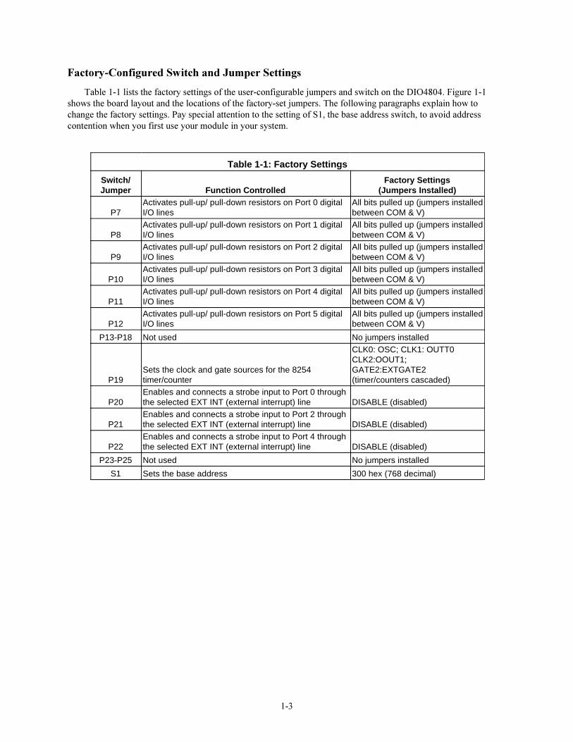
Factory-Configured Switch and Jumper Settings
Table 1-1 lists the factory settings of the user-configurable jumpers and switch on the DIO4804. Figure 1-1shows the board layout and the locations of the factory-set jumpers. The following paragraphs explain how tochange the factory settings. Pay special attention to the setting of S1, the base address switch, to avoid addresscontention when you first use your module in your system.
Table 1-1: Factory Settings
Switch/Jumper Function Controlled
Factory Settings(Jumpers Installed)
P7Activates pull-up/ pull-down resistors on Port 0 digitalI/O lines
All bits pulled up (jumpers installedbetween COM & V)
P8Activates pull-up/ pull-down resistors on Port 1 digitalI/O lines
All bits pulled up (jumpers installedbetween COM & V)
P9Activates pull-up/ pull-down resistors on Port 2 digitalI/O lines
All bits pulled up (jumpers installedbetween COM & V)
P10Activates pull-up/ pull-down resistors on Port 3 digitalI/O lines
All bits pulled up (jumpers installedbetween COM & V)
P11Activates pull-up/ pull-down resistors on Port 4 digitalI/O lines
All bits pulled up (jumpers installedbetween COM & V)
P12Activates pull-up/ pull-down resistors on Port 5 digitalI/O lines
All bits pulled up (jumpers installedbetween COM & V)
P13-P18 Not used No jumpers installed
P19Sets the clock and gate sources for the 8254timer/counter
CLK0: OSC; CLK1: OUTT0CLK2:OOUT1;GATE2:EXTGATE2(timer/counters cascaded)
P20Enables and connects a strobe input to Port 0 throughthe selected EXT INT (external interrupt) line DISABLE (disabled)
P21Enables and connects a strobe input to Port 2 throughthe selected EXT INT (external interrupt) line DISABLE (disabled)
P22Enables and connects a strobe input to Port 4 throughthe selected EXT INT (external interrupt) line DISABLE (disabled)
P23-P25 Not used No jumpers installed
S1 Sets the base address 300 hex (768 decimal)
1-4
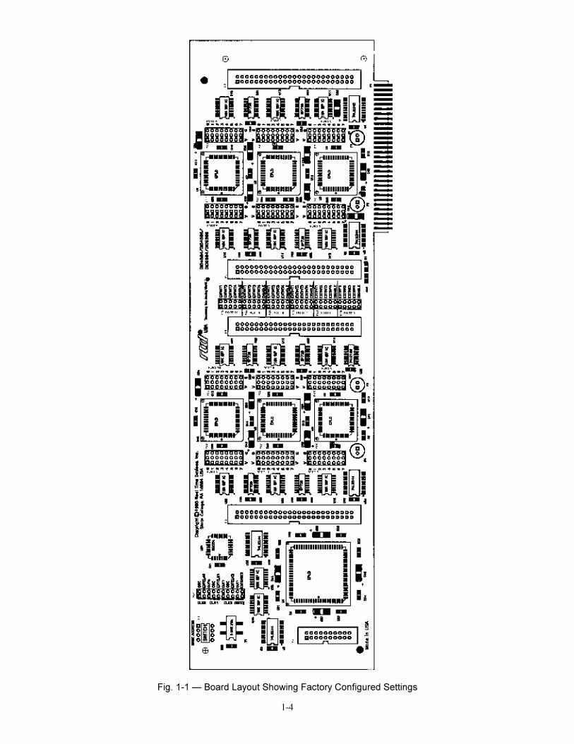
Fig. 1-1 � Board Layout Showing Factory Configured Settings
1-5
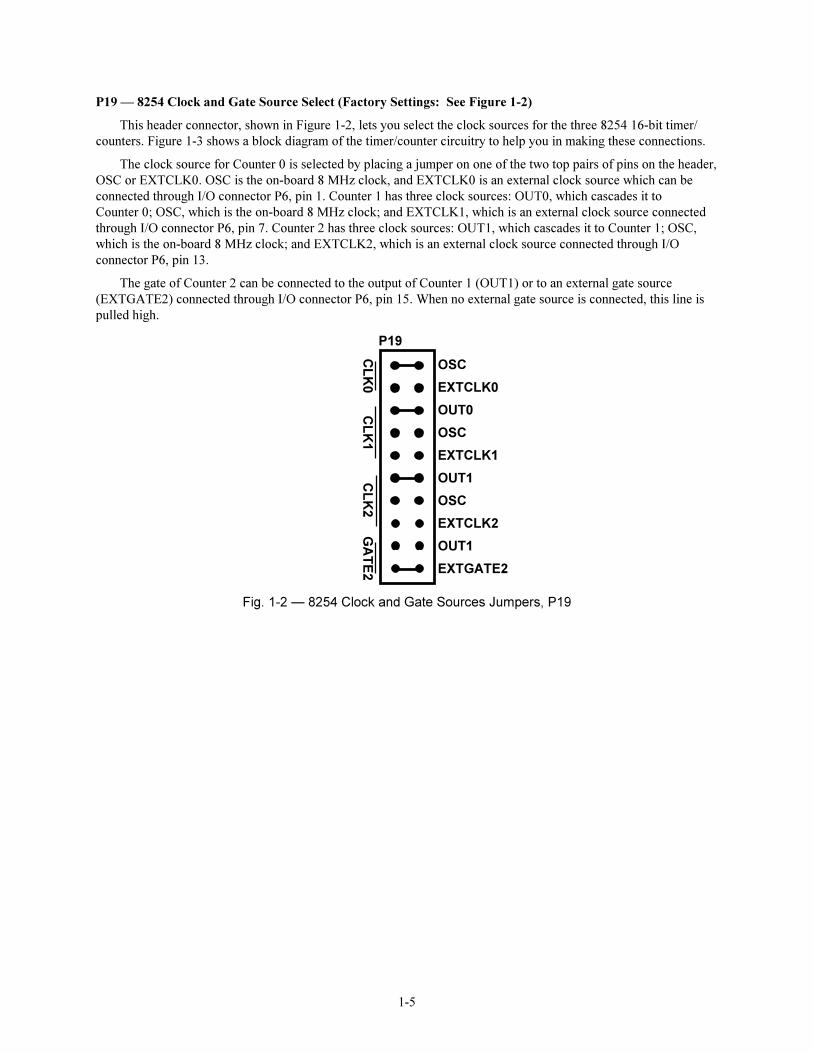
P19 � 8254 Clock and Gate Source Select (Factory Settings: See Figure 1-2)
This header connector, shown in Figure 1-2, lets you select the clock sources for the three 8254 16-bit timer/counters. Figure 1-3 shows a block diagram of the timer/counter circuitry to help you in making these connections.
The clock source for Counter 0 is selected by placing a jumper on one of the two top pairs of pins on the header,OSC or EXTCLK0. OSC is the on-board 8 MHz clock, and EXTCLK0 is an external clock source which can beconnected through I/O connector P6, pin 1. Counter 1 has three clock sources: OUT0, which cascades it toCounter 0; OSC, which is the on-board 8 MHz clock; and EXTCLK1, which is an external clock source connectedthrough I/O connector P6, pin 7. Counter 2 has three clock sources: OUT1, which cascades it to Counter 1; OSC,which is the on-board 8 MHz clock; and EXTCLK2, which is an external clock source connected through I/Oconnector P6, pin 13.
The gate of Counter 2 can be connected to the output of Counter 1 (OUT1) or to an external gate source(EXTGATE2) connected through I/O connector P6, pin 15. When no external gate source is connected, this line ispulled high.
OSC
EXTCLK0
OUT0
OSC
EXTCLK1
OUT1
OSC
EXTCLK2
OUT1
EXTGATE2
GA
TE
2C
LK
2C
LK
1C
LK
0
P19
Fig. 1-2 � 8254 Clock and Gate Sources Jumpers, P19

1-6
P20 through P22 � Strobe Input Enable (Factory Setting: Disabled)
These header connectors connect an external signal (through P2-2, EXTINT1; or P3-2, EXTINT2) to the strobeinput of Port 0, Port 2, and/or Port 4. To enable the strobe input on the digital I/O chip of a selected port, you mustremove the port�s jumper from the DISABLE pins and place it across the desired EXTINT pins. EXTINT3 andEXTINT4 are not connected. Note that multiple ports can be strobed from the same signal. Figure 1-4 shows Port 0,P20. Port 2 is P21 and Port 4 is P22.
CLK1
CLK2
CLK0
ON-BOARDI/O CONNECTOR
P6
PIN 15
PIN 7
PIN 11
8254
TIMER/COUNTER
0CLK
GATE
OUT
TIMER/COUNTER
1CLK
GATE
OUT
TIMER/COUNTER
2CLK
GATE
OUT
PIN 1
PIN 17
XTAL (8 MHz)
P19
+5 V
+5 V
+5 V
PIN 3
PIN 5
PIN 9
PIN 13
T/C OUT 0
OUT0
OUT1
EXT CLK 0
T/C OUT 1
EXT CLK 1
EXT GATE 2
T/C OUT 2
EXT CLK 2
EXT GATE 0
EXT GATE 1
Fig. 1-3 � 8254 Circuit Diagram
Fig. 1-4 � Port 0 Strobe Input Enable Jumper, P20
Fig. 1-4a: Strobe Disabled(Factory Setting)
Fig. 1-4b: Strobe Enabledusing EXTINT1
P20PO
RT
0
EXTINT1
EXTINT2
EXTINT3
EXTINT4
DISABLE
P20PO
RT
0
EXTINT1
EXTINT2
EXTINT3
EXTINT4
DISABLE
1-7
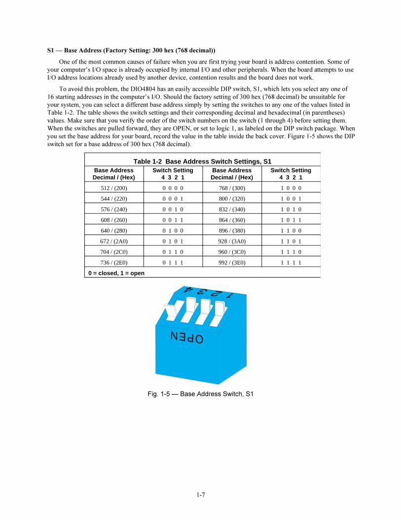
S1 � Base Address (Factory Setting: 300 hex (768 decimal))
One of the most common causes of failure when you are first trying your board is address contention. Some ofyour computer�s I/O space is already occupied by internal I/O and other peripherals. When the board attempts to useI/O address locations already used by another device, contention results and the board does not work.
To avoid this problem, the DIO4804 has an easily accessible DIP switch, S1, which lets you select any one of16 starting addresses in the computer�s I/O. Should the factory setting of 300 hex (768 decimal) be unsuitable foryour system, you can select a different base address simply by setting the switches to any one of the values listed inTable 1-2. The table shows the switch settings and their corresponding decimal and hexadecimal (in parentheses)values. Make sure that you verify the order of the switch numbers on the switch (1 through 4) before setting them.When the switches are pulled forward, they are OPEN, or set to logic 1, as labeled on the DIP switch package. Whenyou set the base address for your board, record the value in the table inside the back cover. Figure 1-5 shows the DIPswitch set for a base address of 300 hex (768 decimal).
Fig. 1-5 � Base Address Switch, S1
Table 1-2 Base Address Switch Settings, S1Base AddressDecimal / (Hex)
Switch Setting4 3 2 1
Base AddressDecimal / (Hex)
Switch Setting4 3 2 1
512 / (200) 0 0 0 0 768 / (300) 1 0 0 0
544 / (220) 0 0 0 1 800 / (320) 1 0 0 1
576 / (240) 0 0 1 0 832 / (340) 1 0 1 0
608 / (260) 0 0 1 1 864 / (360) 1 0 1 1
640 / (280) 0 1 0 0 896 / (380) 1 1 0 0
672 / (2A0) 0 1 0 1 928 / (3A0) 1 1 0 1
704 / (2C0) 0 1 1 0 960 / (3C0) 1 1 1 0
736 / (2E0) 0 1 1 1 992 / (3E0) 1 1 1 1
0 = closed, 1 = open
1-8
0
1
2
3
4
5
6
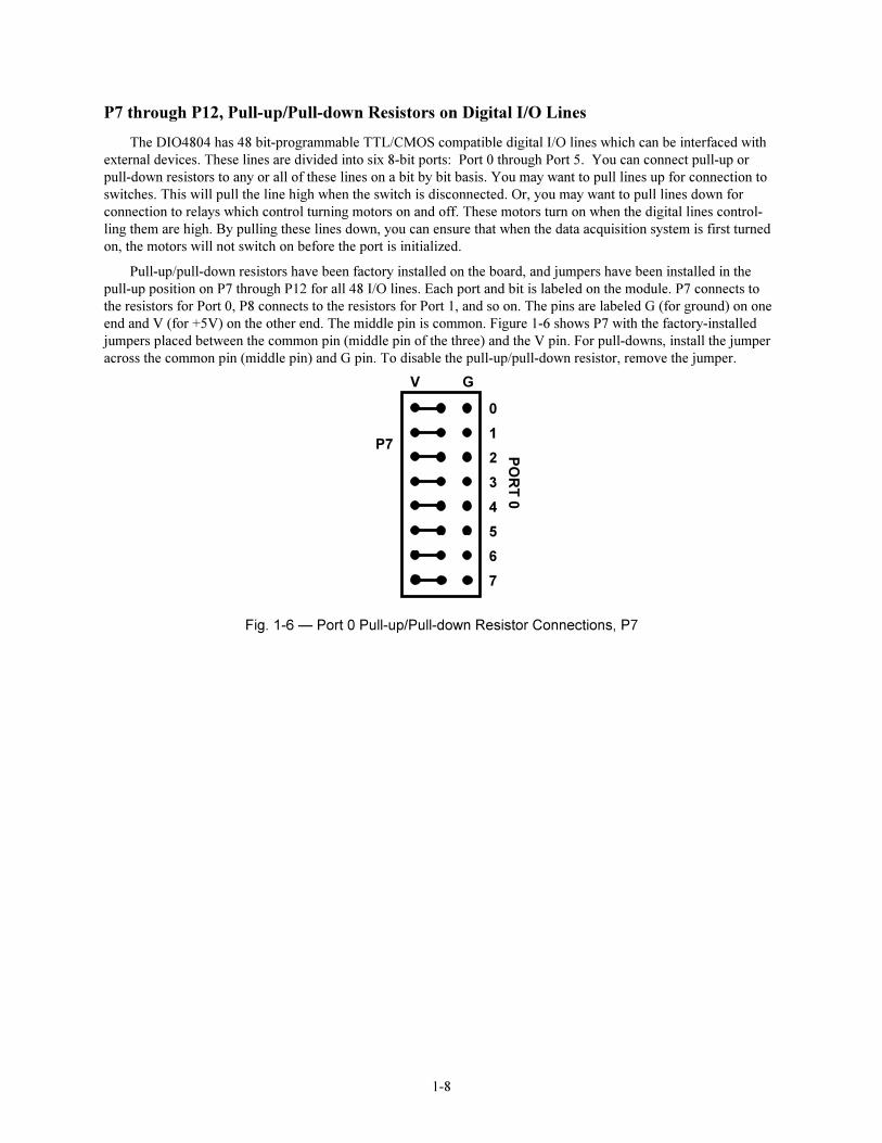
7
P7
V GP
OR
T 0
Fig. 1-6 � Port 0 Pull-up/Pull-down Resistor Connections, P7
P7 through P12, Pull-up/Pull-down Resistors on Digital I/O Lines
The DIO4804 has 48 bit-programmable TTL/CMOS compatible digital I/O lines which can be interfaced withexternal devices. These lines are divided into six 8-bit ports: Port 0 through Port 5. You can connect pull-up orpull-down resistors to any or all of these lines on a bit by bit basis. You may want to pull lines up for connection toswitches. This will pull the line high when the switch is disconnected. Or, you may want to pull lines down forconnection to relays which control turning motors on and off. These motors turn on when the digital lines control-ling them are high. By pulling these lines down, you can ensure that when the data acquisition system is first turnedon, the motors will not switch on before the port is initialized.
Pull-up/pull-down resistors have been factory installed on the board, and jumpers have been installed in thepull-up position on P7 through P12 for all 48 I/O lines. Each port and bit is labeled on the module. P7 connects tothe resistors for Port 0, P8 connects to the resistors for Port 1, and so on. The pins are labeled G (for ground) on oneend and V (for +5V) on the other end. The middle pin is common. Figure 1-6 shows P7 with the factory-installedjumpers placed between the common pin (middle pin of the three) and the V pin. For pull-downs, install the jumperacross the common pin (middle pin) and G pin. To disable the pull-up/pull-down resistor, remove the jumper.
2-1
CHAPTER 2
BOARD INSTALLATION
The DIO4804 is easy to install in your PC. This chapter tellsyou step-by-step how to install and connect the board.
After you have installed the board and made all of your con-nections, you can turn your system on and run the 4804DIAGboard diagnostics program included on your example software diskto verify that your board is working.

2-2
2-3
Board Installation
Keep the board in its antistatic bag until you are ready to install it in your computer. When removing it from thebag, hold the board at the edges and do not touch the components or connectors.
Before installing the board in your computer, check the jumper and switch settings. Chapter 1 reviews thefactory settings and how to change them. If you need to change any settings, refer to the appropriate instructions inChapter 1. Note that incompatible jumper settings can result in unpredictable board operation and erratic response.
To install the board:
1. Turn OFF the power to your computer.
2. Remove the top cover of the computer housing (refer to your owner�s manual if you do not already knowhow to do this).
3. Select any unused full-size expansion slot and remove the slot bracket.
4. Touch the metal housing of the computer to discharge any static buildup and then remove the board from itsantistatic bag.
5. Holding the board by its edges, orient it so that its card edge (bus) connector lines up with the expansion slotconnector in the bottom of the selected expansion slot.
5. Before placing the board into the computer, the two 50-pin ribbon cable assemblies must be installed onboard connectors P2 and P3, and, if you are using the 8254 timer/counter, a 20-pin cable assembly must beinstalled on P6. If you have purchased the DIO4804 cable set, first install the P2 cable on connector P2. Theninstall the P3 cable on P3, and, if needed, the P6 cable on P6. Each cable is brought out through a singleconnector slot in the rear panel of the computer. To install the cables:
a. Remove the strain relief clamp attached to the DIO4804 bracket located on the right side ofthe board.
b. Connect the socket connector to the board connector for each cable. When installing, observethe connector keying and press firmly to make sure that the socket connector is fully seatedon the board. Each cable provided is labeled with the connector's P number for easyidentification. The cables have strain reliefs on one connector and not on the other. Theconnector without the strain relief is to be installed on the board. After the cables are installedon the board, position them so that they pass over the flange in the board�s bracket.
c. Re-attach the clamp to the bracket using the hardware supplied with your DIO4804, securingthe ribbon cables in place.
6. After checking that the cables are correctly installed on the board, orient the board inside the computer so thatthe cables extend through the rear panel opening and the card edge connector lines up with the expansion slotconnector. Then, press down on the metal bracket tab and the top of the board until the board is firmly seatedin the expansion slot connector.
NOTE: Do not force the board into the slot. If the board does not slide into place, remove it and try again.Wiggling the board or exerting too much pressure can result in damage to the board or to the computer.
7. After the board is installed, secure the slot bracket back into place and put the cover back on your computer.The board is now ready to be connected via the external I/O connector at the rear panel of your computer.
External I/O Connections
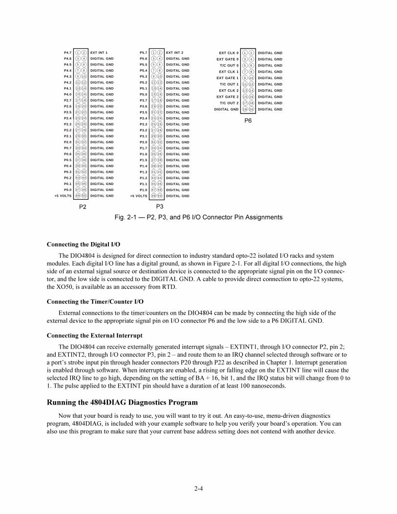
Figure 2-1 shows I/O connector pinouts for the digital I/O connectors. Refer to these diagrams as you makeyour I/O connections.
2-4
Fig. 2-1 � P2, P3, and P6 I/O Connector Pin Assignments
3 9 4 0
3 7 3 8
3 5 3 6
3 3 3 4
3 1 3 2
2 9 3 0
2 7 2 8
2 5 2 6
2 3 2 4
2 1 2 2
1 9 2 0
1 7 1 8
1 5 1 6
1 3 1 4
11 1 2
9 1 0
7 8
5 6
3 4
1 2
4 9 5 0
4 7 4 8
4 5 4 6
4 3 4 4
4 1 4 2
P4.7
P4.6
P4.5
P4.4
P4.3
P4.2
P4.1
P4.0
P2.7
P2.6
P2.5
P2.4
P2.3
P2.2
P2.1
P2.0
P0.7
P0.6
P0.5
P0.4
P0.3
P0.2
P0.1
P0.0
+5 VOLTS
EXT INT 1
DIGITAL GND
DIGITAL GND
DIGITAL GND
DIGITAL GND
DIGITAL GND
DIGITAL GND
DIGITAL GND
DIGITAL GND
DIGITAL GND
DIGITAL GND
DIGITAL GND
DIGITAL GND
DIGITAL GND
DIGITAL GND
DIGITAL GND
DIGITAL GND
DIGITAL GND
DIGITAL GND
DIGITAL GND
DIGITAL GND
DIGITAL GND
DIGITAL GND
DIGITAL GND
DIGITAL GND
3 9 4 0
3 7 3 8
3 5 3 6
3 3 3 4
3 1 3 2
2 9 3 0
2 7 2 8
2 5 2 6
2 3 2 4
2 1 2 2
1 9 2 0
1 7 1 8
1 5 1 6
1 3 1 4
11 1 2
9 1 0
7 8
5 6
3 4
1 2
4 9 5 0
4 7 4 8
4 5 4 6
4 3 4 4
4 1 4 2
P5.7
P5.6
P5.5
P5.4
P5.3
P5.2
P5.1
P5.0
P3.7
P3.6
P3.5
P3.4
P3.3
P3.2
P3.1
P3.0
P1.7
P1.6
P1.5
P1.4
P1.3
P1.2
P1.1
P1.0
+5 VOLTS
EXT INT 2
DIGITAL GND
DIGITAL GND
DIGITAL GND
DIGITAL GND
DIGITAL GND
DIGITAL GND
DIGITAL GND
DIGITAL GND
DIGITAL GND
DIGITAL GND
DIGITAL GND
DIGITAL GND
DIGITAL GND
DIGITAL GND
DIGITAL GND
DIGITAL GND
DIGITAL GND
DIGITAL GND
DIGITAL GND
DIGITAL GND
DIGITAL GND
DIGITAL GND
DIGITAL GND
DIGITAL GND
P3P2
1 9 2 0
1 7 1 8
1 5 1 6
1 3 1 4
11 1 2
9 1 0
7 8
5 6
3 4
1 2EXT CLK 0
EXT GATE 0
T/C OUT 0
EXT CLK 1
EXT GATE 1
T/C OUT 1
EXT CLK 2
EXT GATE 2
T/C OUT 2
DIGITAL GND
DIGITAL GND
DIGITAL GND
DIGITAL GND
DIGITAL GND
DIGITAL GND
DIGITAL GND
DIGITAL GND
DIGITAL GND
DIGITAL GND
DIGITAL GND
P6
Connecting the Digital I/O
The DIO4804 is designed for direct connection to industry standard opto-22 isolated I/O racks and systemmodules. Each digital I/O line has a digital ground, as shown in Figure 2-1. For all digital I/O connections, the highside of an external signal source or destination device is connected to the appropriate signal pin on the I/O connec-tor, and the low side is connected to the DIGITAL GND. A cable to provide direct connection to opto-22 systems,the XO50, is available as an accessory from RTD.
Connecting the Timer/Counter I/O
External connections to the timer/counters on the DIO4804 can be made by connecting the high side of theexternal device to the appropriate signal pin on I/O connector P6 and the low side to a P6 DIGITAL GND.
Connecting the External Interrupt
The DIO4804 can receive externally generated interrupt signals � EXTINT1, through I/O connector P2, pin 2;and EXTINT2, through I/O connector P3, pin 2 � and route them to an IRQ channel selected through software or toa port�s strobe input pin through header connectors P20 through P22 as described in Chapter 1. Interrupt generationis enabled through software. When interrupts are enabled, a rising or falling edge on the EXTINT line will cause theselected IRQ line to go high, depending on the setting of BA + 16, bit 1, and the IRQ status bit will change from 0 to1. The pulse applied to the EXTINT pin should have a duration of at least 100 nanoseconds.
Running the 4804DIAG Diagnostics Program
Now that your board is ready to use, you will want to try it out. An easy-to-use, menu-driven diagnosticsprogram, 4804DIAG, is included with your example software to help you verify your board�s operation. You canalso use this program to make sure that your current base address setting does not contend with another device.
3-1
CHAPTER 3
HARDWARE DESCRIPTION
This chapter describes the features of the DIO4804 hardware.The major circuits are the digital I/O lines and the timer/counters.

3-2
3-3
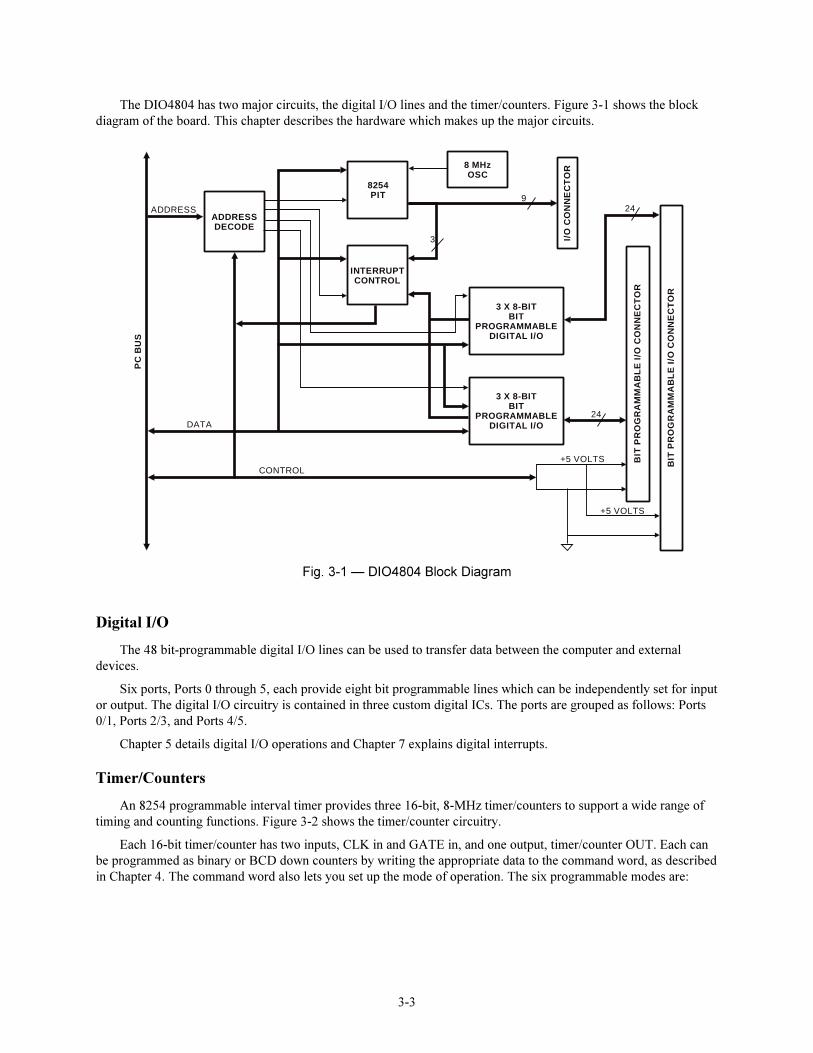
The DIO4804 has two major circuits, the digital I/O lines and the timer/counters. Figure 3-1 shows the blockdiagram of the board. This chapter describes the hardware which makes up the major circuits.
Digital I/O
The 48 bit-programmable digital I/O lines can be used to transfer data between the computer and externaldevices.
Six ports, Ports 0 through 5, each provide eight bit programmable lines which can be independently set for inputor output. The digital I/O circuitry is contained in three custom digital ICs. The ports are grouped as follows: Ports0/1, Ports 2/3, and Ports 4/5.
Chapter 5 details digital I/O operations and Chapter 7 explains digital interrupts.
Timer/Counters
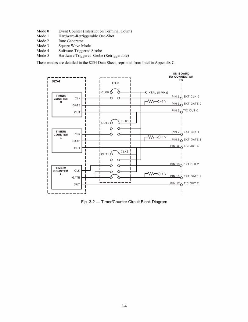
An 8254 programmable interval timer provides three 16-bit, 8-MHz timer/counters to support a wide range oftiming and counting functions. Figure 3-2 shows the timer/counter circuitry.
Each 16-bit timer/counter has two inputs, CLK in and GATE in, and one output, timer/counter OUT. Each canbe programmed as binary or BCD down counters by writing the appropriate data to the command word, as describedin Chapter 4. The command word also lets you set up the mode of operation. The six programmable modes are:
Fig. 3-1 � DIO4804 Block Diagram
+5 VOLTS
24
ADDRESSDECODE
INTERRUPTCONTROL
ADDRESS
DATA
CONTROL
PC
BU
S
3 X 8-BITBIT
PROGRAMMABLEDIGITAL I/O
8254PIT
8 MHzOSC
9
3
BIT
PR
OG
RA
MM
AB
LE
I/O
CO
NN
EC
TO
R
I/O
CO
NN
EC
TO
R
24
3 X 8-BITBIT
PROGRAMMABLEDIGITAL I/O
+5 VOLTS
BIT
PR
OG
RA
MM
AB
LE
I/O
CO
NN
EC
TO
R
3-4
Mode 0 Event Counter (Interrupt on Terminal Count)Mode 1 Hardware-Retriggerable One-ShotMode 2 Rate GeneratorMode 3 Square Wave ModeMode 4 Software-Triggered StrobeMode 5 Hardware Triggered Strobe (Retriggerable)
These modes are detailed in the 8254 Data Sheet, reprinted from Intel in Appendix C.
CLK1
CLK2
CLK0
ON-BOARDI/O CONNECTOR
P6
PIN 15
PIN 7
PIN 11
8254
TIMER/COUNTER
0CLK
GATE
OUT
TIMER/COUNTER
1CLK
GATE
OUT
TIMER/COUNTER
2CLK
GATE
OUT
PIN 1
PIN 17
XTAL (8 MHz)
P19
+5 V
+5 V
+5 V
PIN 3
PIN 5
PIN 9
PIN 13
T/C OUT 0
OUT0
OUT1
EXT CLK 0
T/C OUT 1
EXT CLK 1
EXT GATE 2
T/C OUT 2
EXT CLK 2
EXT GATE 0
EXT GATE 1
Fig. 3-2 � Timer/Counter Circuit Block Diagram
4-1
CHAPTER 4
I/O MAPPING
This chapter provides a complete description of the I/O map forthe DIO4804, general programming information, and how to setand clear bits in a port.

4-2
4-3
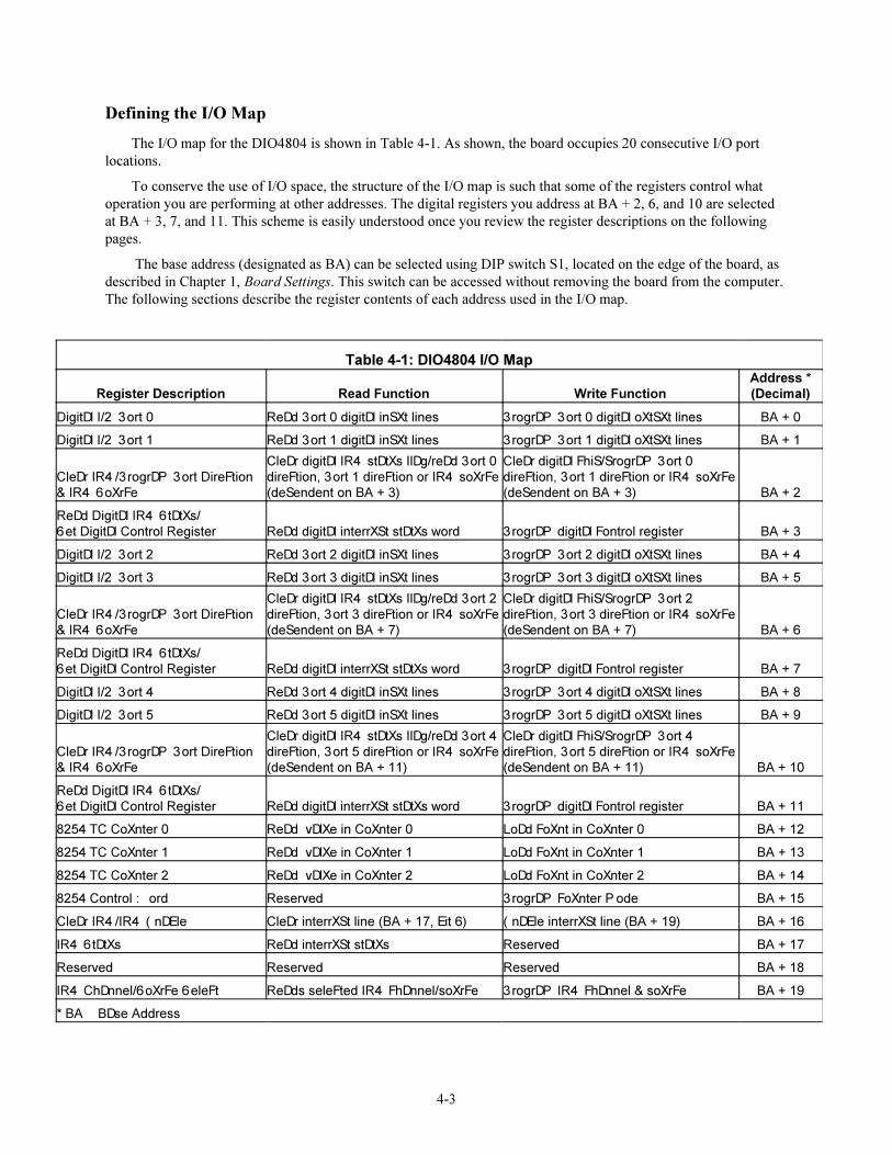
Defining the I/O Map
The I/O map for the DIO4804 is shown in Table 4-1. As shown, the board occupies 20 consecutive I/O portlocations.
To conserve the use of I/O space, the structure of the I/O map is such that some of the registers control whatoperation you are performing at other addresses. The digital registers you address at BA + 2, 6, and 10 are selectedat BA + 3, 7, and 11. This scheme is easily understood once you review the register descriptions on the followingpages.
The base address (designated as BA) can be selected using DIP switch S1, located on the edge of the board, asdescribed in Chapter 1, Board Settings. This switch can be accessed without removing the board from the computer.The following sections describe the register contents of each address used in the I/O map.
7DEOH������',2�����,�2�0DS
5HJLVWHU�'HVFULSWLRQ 5HDG�)XQFWLRQ :ULWH�)XQFWLRQ$GGUHVV� �'HFLPDO�
' LJLWDO�,�2 �3RUW�� 5 HDG�3RUW���GLJLWDO�LQSXW�OLQHV 3URJUDP �3RUW���GLJLWDO�RXWSXW�OLQHV %$����
' LJLWDO�,�2 �3RUW�� 5 HDG�3RUW���GLJLWDO�LQSXW�OLQHV 3URJUDP �3RUW���GLJLWDO�RXWSXW�OLQHV %$����
&OHDU�,5 4 �3URJUDP �3RUW�' LUHFWLRQ�,5 4 �6RXUFH
&OHDU�GLJLWDO�,5 4 �VWDWXV�IODJ�UHDG�3RUW��GLUHFWLRQ��3RUW���GLUHFWLRQ�RU�,5 4 �VRXUFH�GHSHQGHQW�RQ�%$�����
&OHDU�GLJLWDO�FKLS�SURJUDP �3RUW��GLUHFWLRQ��3RUW���GLUHFWLRQ�RU�,5 4 �VRXUFH�GHSHQGHQW�RQ�%$����� %$����
5 HDG�' LJLWDO�,5 4 �6WDWXV�6HW�' LJLWDO�&RQWURO�5 HJLVWHU 5 HDG�GLJLWDO�LQWHUUXSW�VWDWXV�ZRUG 3URJUDP �GLJLWDO�FRQWURO�UHJLVWHU %$����
' LJLWDO�,�2 �3RUW�� 5 HDG�3RUW���GLJLWDO�LQSXW�OLQHV 3URJUDP �3RUW���GLJLWDO�RXWSXW�OLQHV %$����
' LJLWDO�,�2 �3RUW�� 5 HDG�3RUW���GLJLWDO�LQSXW�OLQHV 3URJUDP �3RUW���GLJLWDO�RXWSXW�OLQHV %$����
&OHDU�,5 4 �3URJUDP �3RUW�' LUHFWLRQ�,5 4 �6RXUFH
&OHDU�GLJLWDO�,5 4 �VWDWXV�IODJ�UHDG�3RUW��GLUHFWLRQ��3RUW���GLUHFWLRQ�RU�,5 4 �VRXUFH�GHSHQGHQW�RQ�%$������
&OHDU�GLJLWDO�FKLS�SURJUDP �3RUW��GLUHFWLRQ��3RUW���GLUHFWLRQ�RU�,5 4 �VRXUFH�GHSHQGHQW�RQ�%$������ %$�����
5 HDG�' LJLWDO�,5 4 �6WDWXV�6HW�' LJLWDO�&RQWURO�5 HJLVWHU 5 HDG�GLJLWDO�LQWHUUXSW�VWDWXV�ZRUG 3URJUDP �GLJLWDO�FRQWURO�UHJLVWHU %$�����
�����7&�&RXQWHU�� 5 HDG��YDOXH�LQ�&RXQWHU�� / RDG�FRXQW�LQ�&RXQWHU�� %$�����
�����7&�&RXQWHU�� 5 HDG��YDOXH�LQ�&RXQWHU�� / RDG�FRXQW�LQ�&RXQWHU�� %$�����
�����7&�&RXQWHU�� 5 HDG��YDOXH�LQ�&RXQWHU�� / RDG�FRXQW�LQ�&RXQWHU�� %$�����
�����&RQWURO�: RUG 5 HVHUYHG 3URJUDP �FRXQWHU�P RGH %$�����
&OHDU�,5 4 �,5 4 �( QDEOH &OHDU�LQWHUUXSW�OLQH��%$�������ELW��� ( QDEOH�LQWHUUXSW�OLQH��%$������ %$�����
,5 4 �6WDWXV 5 HDG�LQWHUUXSW�VWDWXV 5 HVHUYHG %$�����
5 HVHUYHG 5 HVHUYHG 5 HVHUYHG %$�����
,5 4 �&KDQQHO�6RXUFH�6HOHFW 5 HDGV�VHOHFWHG�,5 4 �FKDQQHO�VRXUFH 3URJUDP �,5 4 �FKDQQHO��VRXUFH %$�����
�%$� �%DVH�$GGUHVV

4-4
BA + 0: Digital I/O Port 0 (Read/Write)
This port transfers the 8-bit Port 0 bit programmable digital input/output data between the board and externaldevices. The bits are individually programmed as input or output by writing to the Port 0 Direction Register atBA + 2. For all bits set as inputs, a read reads the input values and a write is ignored. For all bits set as outputs, aread reads the last value sent out on the line and a write writes the current loaded value out to the line.
Note that when any reset of the digital circuitry is performed (clear chip or computer reset), all digital lines arereset to inputs and their corresponding output registers are cleared.
BA + 1: Digital I/O Port 1 (Read/Write)
This port transfers the 8-bit Port 1 bit programmable digital input/output data between the board and externaldevices. The bits are individually programmed as input or output by writing to the Port 1 Direction Register atBA + 2. For all bits set as inputs, a read reads the input values and a write is ignored. For all bits set as outputs, aread reads the last value sent out on the line and a write writes the current loaded value out to the line.
Note that when any reset of the digital circuitry is performed (clear chip or computer reset ), all digital lines arereset to inputs and their corresponding output registers are cleared.
D7 D6 D5 D4 D3 D2 D1 D0P0.7 P0.6 P0.5 P0.4 P0.3 P0.2 P0.1 P0.0
D7 D6 D5 D4 D3 D2 D1 D0P1.7 P1.6 P1.5 P1.4 P1.3 P1.2 P1.1 P1.0
BA + 2: Clear IRQ/Program Port 0 Direction/Port 1 Direction/IRQ Source Registers (Read/Write)
A read clears the IRQ status flag or provides the contents of one of three control registers: Port 0 Direction, Port1 Direction, or Port 0/1 custom digital IC IRQ Source. A write clears the digital chip or programs one of the threecontrol registers, depending on the setting of bits 1 and 0 at BA + 3. When bits 1 and 0 at BA + 3 are 00, the read/write operations clear the digital IRQ status flag (read) and the digital chip (write). When these bits are set to anyother value, one of the three Port 0/1 digital I/O registers is addressed.
Port 0 Direction Register (BA + 3, bits 1 and 0 = 01):
D7 D6 D5 D4 D3 D2 D1 D0P0.7 P0.6 P0.5 P0.4 P0.3 P0.2 P0.1 P0.0
For all bits:0 = input1 = output
This register programs the direction, input or output, of each bit at Port 0.
Port 1 Direction Register (BA + 3, bits 1 and 0 = 10):
D7 D6 D5 D4 D3 D2 D1 D0P1.7 P1.6 P1.5 P1.4 P1.3 P1.2 P1.1 P1.0
For all bits:0 = input1 = output
This register programs the direction, input or output, of each bit at Port 1.
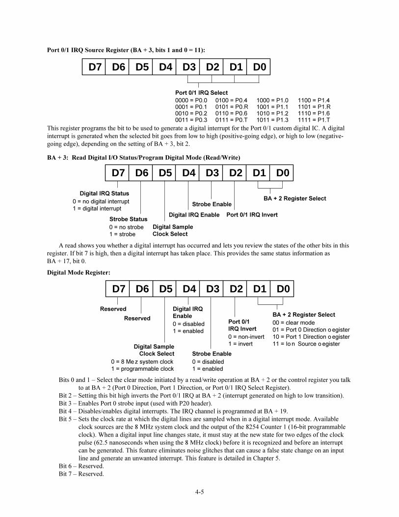
4-5
D7 D6 D5 D4 D3 D2 D1 D0
BA + 2 Register Select
Digital SampleClock Select
Digital IRQ Status0 = no digital interrupt1 = digital interrupt
Strobe Status0 = no strobe1 = strobe
Digital IRQ Enable
Strobe Enable
Port 0/1 IRQ Invert
D7 D6 D5 D4 D3 D2 D1 D0
Port 0/1 IRQ Select0000 = P0.00001 = P0.10010 = P0.20011 = P0.3
0100 = P0.40101 = P0.50110 = P0.60111 = P0.7
1000 = P1.01001 = P1.11010 = P1.21011 = P1.3
1100 = P1.41101 = P1.51110 = P1.61111 = P1.7
Bits 0 and 1 � Select the clear mode initiated by a read/write operation at BA + 2 or the control register you talkto at BA + 2 (Port 0 Direction, Port 1 Direction, or Port 0/1 IRQ Select Register).
Bit 2 � Setting this bit high inverts the Port 0/1 IRQ at BA + 2 (interrupt generated on high to low transition).Bit 3 � Enables Port 0 strobe input (used with P20 header).Bit 4 � Disables/enables digital interrupts. The IRQ channel is programmed at BA + 19.Bit 5 � Sets the clock rate at which the digital lines are sampled when in a digital interrupt mode. Available
clock sources are the 8 MHz system clock and the output of the 8254 Counter 1 (16-bit programmableclock). When a digital input line changes state, it must stay at the new state for two edges of the clockpulse (62.5 nanoseconds when using the 8 MHz clock) before it is recognized and before an interruptcan be generated. This feature eliminates noise glitches that can cause a false state change on an inputline and generate an unwanted interrupt. This feature is detailed in Chapter 5.
Bit 6 � Reserved.Bit 7 � Reserved.
D7 D6 D5 D4 D3 D2 D1 D0
Reserved
ReservedBA + 2 Register Select00 = clear mode01 = Port 0 Direction Register10 = Port 1 Direction Register11 = IRQ Source Register
Strobe Enable0 = disabled1 = enabled
Digital SampleClock Select
0 = 8 MHz system clock1 = programmable clock
Port 0/1IRQ Invert0 = non-invert1 = invert
Digital IRQEnable0 = disabled1 = enabled
Port 0/1 IRQ Source Register (BA + 3, bits 1 and 0 = 11):
This register programs the bit to be used to generate a digital interrupt for the Port 0/1 custom digital IC. A digitalinterrupt is generated when the selected bit goes from low to high (positive-going edge), or high to low (negative-going edge), depending on the setting of BA + 3, bit 2.
BA + 3: Read Digital I/O Status/Program Digital Mode (Read/Write)
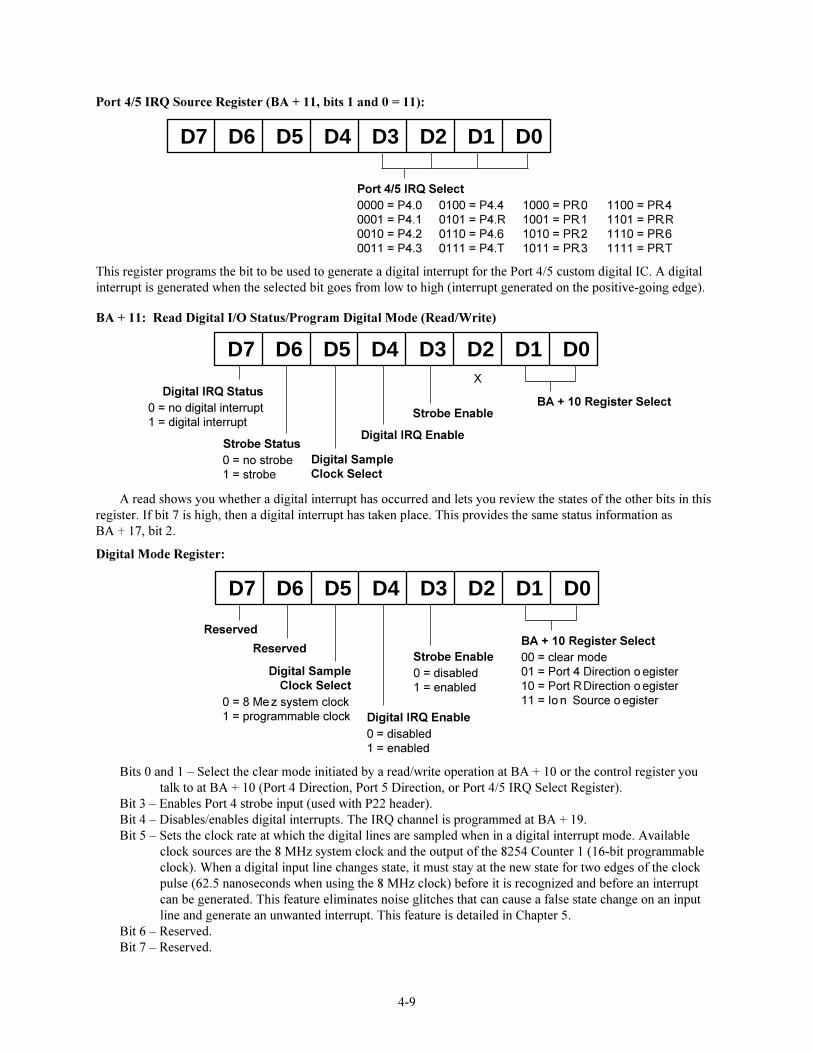
A read shows you whether a digital interrupt has occurred and lets you review the states of the other bits in thisregister. If bit 7 is high, then a digital interrupt has taken place. This provides the same status information asBA + 17, bit 0.
Digital Mode Register:
4-6
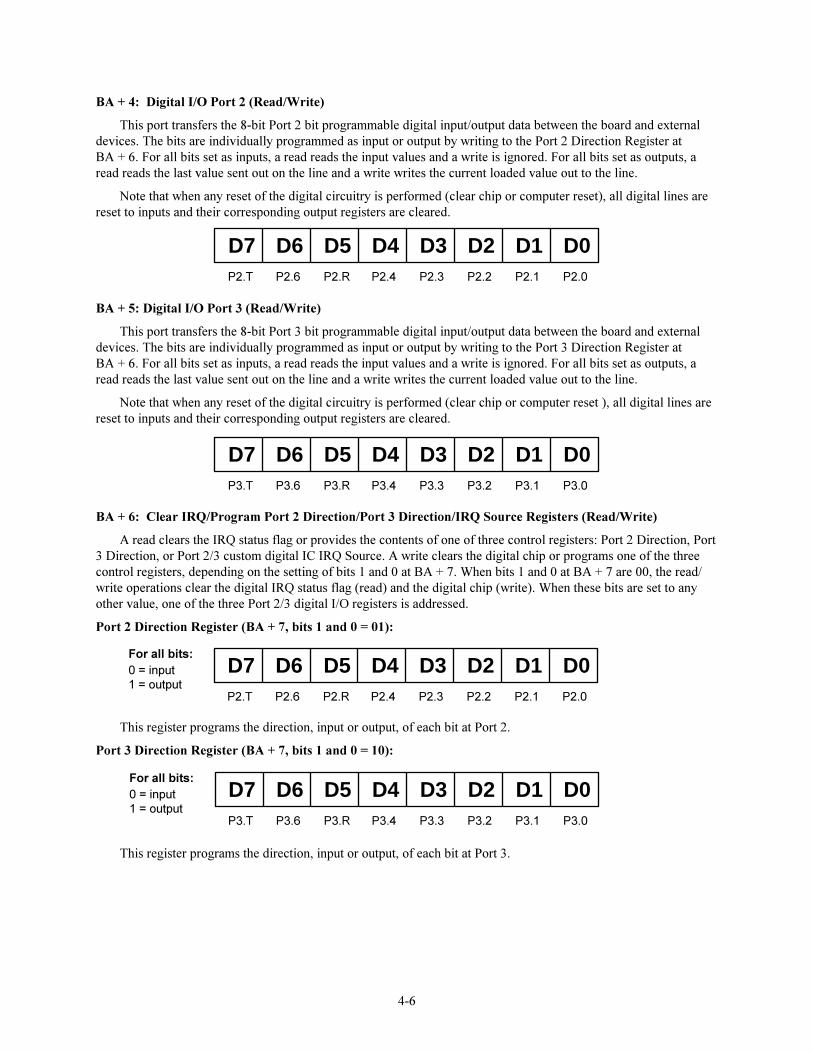
BA + 4: Digital I/O Port 2 (Read/Write)
This port transfers the 8-bit Port 2 bit programmable digital input/output data between the board and externaldevices. The bits are individually programmed as input or output by writing to the Port 2 Direction Register atBA + 6. For all bits set as inputs, a read reads the input values and a write is ignored. For all bits set as outputs, aread reads the last value sent out on the line and a write writes the current loaded value out to the line.
Note that when any reset of the digital circuitry is performed (clear chip or computer reset), all digital lines arereset to inputs and their corresponding output registers are cleared.
BA + 6: Clear IRQ/Program Port 2 Direction/Port 3 Direction/IRQ Source Registers (Read/Write)
A read clears the IRQ status flag or provides the contents of one of three control registers: Port 2 Direction, Port3 Direction, or Port 2/3 custom digital IC IRQ Source. A write clears the digital chip or programs one of the threecontrol registers, depending on the setting of bits 1 and 0 at BA + 7. When bits 1 and 0 at BA + 7 are 00, the read/write operations clear the digital IRQ status flag (read) and the digital chip (write). When these bits are set to anyother value, one of the three Port 2/3 digital I/O registers is addressed.
Port 2 Direction Register (BA + 7, bits 1 and 0 = 01):
D7 D6 D5 D4 D3 D2 D1 D0P2.7 P2.6 P2.5 P2.4 P2.3 P2.2 P2.1 P2.0
D7 D6 D5 D4 D3 D2 D1 D0P3.7 P3.6 P3.5 P3.4 P3.3 P3.2 P3.1 P3.0
D7 D6 D5 D4 D3 D2 D1 D0P2.7 P2.6 P2.5 P2.4 P2.3 P2.2 P2.1 P2.0
For all bits:0 = input1 = output
D7 D6 D5 D4 D3 D2 D1 D0P3.7 P3.6 P3.5 P3.4 P3.3 P3.2 P3.1 P3.0
For all bits:0 = input1 = output
BA + 5: Digital I/O Port 3 (Read/Write)
This port transfers the 8-bit Port 3 bit programmable digital input/output data between the board and externaldevices. The bits are individually programmed as input or output by writing to the Port 3 Direction Register atBA + 6. For all bits set as inputs, a read reads the input values and a write is ignored. For all bits set as outputs, aread reads the last value sent out on the line and a write writes the current loaded value out to the line.
Note that when any reset of the digital circuitry is performed (clear chip or computer reset ), all digital lines arereset to inputs and their corresponding output registers are cleared.
This register programs the direction, input or output, of each bit at Port 2.
Port 3 Direction Register (BA + 7, bits 1 and 0 = 10):
This register programs the direction, input or output, of each bit at Port 3.
4-7
0100 = P2.40101 = P2.50110 = P2.60111 = P2.7
D7 D6 D5 D4 D3 D2 D1 D0
Port 2/3 IRQ Select0000 = P2.00001 = P2.10010 = P2.20011 = P2.3
1000 = P3.01001 = P3.11010 = P3.21011 = P3.3
1100 = P3.41101 = P3.51110 = P3.61111 = P3.7
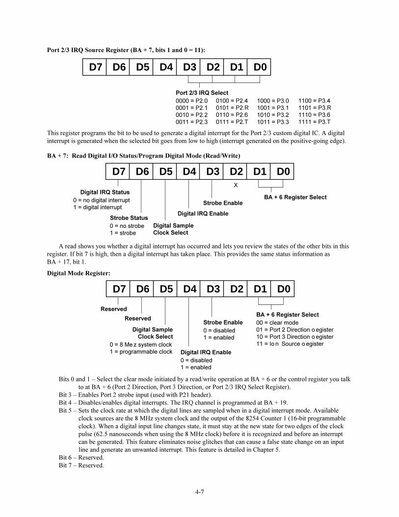
Port 2/3 IRQ Source Register (BA + 7, bits 1 and 0 = 11):
D7 D6 D5 D4 D3 D2 D1 D0
D7 D6 D5 D4 D3 D2 D1 D0
BA + 6 Register SelectStrobe Enable
Digital IRQ Enable
Digital SampleClock Select
Digital IRQ Status0 = no digital interrupt1 = digital interrupt
Strobe Status0 = no strobe1 = strobe
BA + 6 Register Select00 = clear mode01 = Port 2 Direction Register10 = Port 3 Direction Register11 = IRQ Source Register
Strobe Enable0 = disabled1 = enabled
Digital IRQ Enable0 = disabled1 = enabled
Reserved
Reserved
Digital SampleClock Select
0 = 8 MHz system clock1 = programmable clock
This register programs the bit to be used to generate a digital interrupt for the Port 2/3 custom digital IC. A digitalinterrupt is generated when the selected bit goes from low to high (interrupt generated on the positive-going edge).
BA + 7: Read Digital I/O Status/Program Digital Mode (Read/Write)
A read shows you whether a digital interrupt has occurred and lets you review the states of the other bits in thisregister. If bit 7 is high, then a digital interrupt has taken place. This provides the same status information asBA + 17, bit 1.
Digital Mode Register:
Bits 0 and 1 � Select the clear mode initiated by a read/write operation at BA + 6 or the control register you talkto at BA + 6 (Port 2 Direction, Port 3 Direction, or Port 2/3 IRQ Select Register).
Bit 3 � Enables Port 2 strobe input (used with P21 header).Bit 4 � Disables/enables digital interrupts. The IRQ channel is programmed at BA + 19.Bit 5 � Sets the clock rate at which the digital lines are sampled when in a digital interrupt mode. Available
clock sources are the 8 MHz system clock and the output of the 8254 Counter 1 (16-bit programmableclock). When a digital input line changes state, it must stay at the new state for two edges of the clockpulse (62.5 nanoseconds when using the 8 MHz clock) before it is recognized and before an interruptcan be generated. This feature eliminates noise glitches that can cause a false state change on an inputline and generate an unwanted interrupt. This feature is detailed in Chapter 5.
Bit 6 � Reserved.Bit 7 � Reserved.
X
4-8
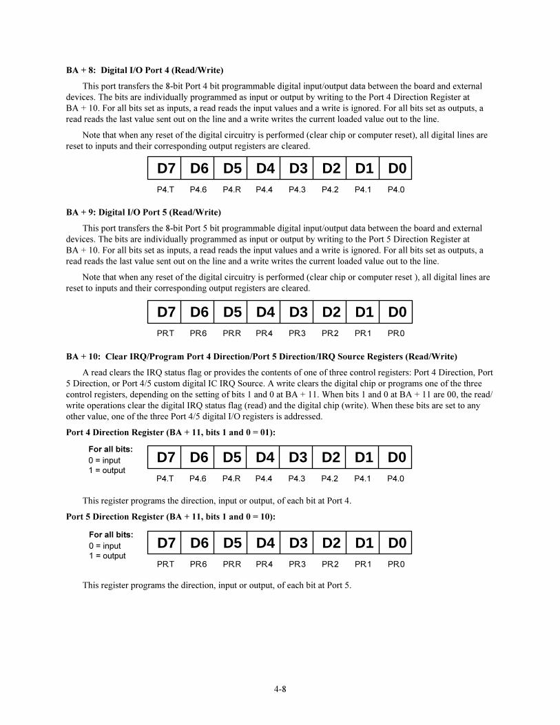
BA + 8: Digital I/O Port 4 (Read/Write)
This port transfers the 8-bit Port 4 bit programmable digital input/output data between the board and externaldevices. The bits are individually programmed as input or output by writing to the Port 4 Direction Register atBA + 10. For all bits set as inputs, a read reads the input values and a write is ignored. For all bits set as outputs, aread reads the last value sent out on the line and a write writes the current loaded value out to the line.
Note that when any reset of the digital circuitry is performed (clear chip or computer reset), all digital lines arereset to inputs and their corresponding output registers are cleared.
D7 D6 D5 D4 D3 D2 D1 D0P4.7 P4.6 P4.5 P4.4 P4.3 P4.2 P4.1 P4.0
D7 D6 D5 D4 D3 D2 D1 D0P5.7 P5.6 P5.5 P5.4 P5.3 P5.2 P5.1 P5.0
D7 D6 D5 D4 D3 D2 D1 D0P4.7 P4.6 P4.5 P4.4 P4.3 P4.2 P4.1 P4.0
For all bits:0 = input1 = output
D7 D6 D5 D4 D3 D2 D1 D0P5.7 P5.6 P5.5 P5.4 P5.3 P5.2 P5.1 P5.0
For all bits:0 = input1 = output
BA + 9: Digital I/O Port 5 (Read/Write)
This port transfers the 8-bit Port 5 bit programmable digital input/output data between the board and externaldevices. The bits are individually programmed as input or output by writing to the Port 5 Direction Register atBA + 10. For all bits set as inputs, a read reads the input values and a write is ignored. For all bits set as outputs, aread reads the last value sent out on the line and a write writes the current loaded value out to the line.
Note that when any reset of the digital circuitry is performed (clear chip or computer reset ), all digital lines arereset to inputs and their corresponding output registers are cleared.
BA + 10: Clear IRQ/Program Port 4 Direction/Port 5 Direction/IRQ Source Registers (Read/Write)
A read clears the IRQ status flag or provides the contents of one of three control registers: Port 4 Direction, Port5 Direction, or Port 4/5 custom digital IC IRQ Source. A write clears the digital chip or programs one of the threecontrol registers, depending on the setting of bits 1 and 0 at BA + 11. When bits 1 and 0 at BA + 11 are 00, the read/write operations clear the digital IRQ status flag (read) and the digital chip (write). When these bits are set to anyother value, one of the three Port 4/5 digital I/O registers is addressed.
Port 4 Direction Register (BA + 11, bits 1 and 0 = 01):
This register programs the direction, input or output, of each bit at Port 4.
Port 5 Direction Register (BA + 11, bits 1 and 0 = 10):
This register programs the direction, input or output, of each bit at Port 5.
4-9
0100 = P4.40101 = P4.50110 = P4.60111 = P4.7
D7 D6 D5 D4 D3 D2 D1 D0
Port 4/5 IRQ Select0000 = P4.00001 = P4.10010 = P4.20011 = P4.3
1000 = P5.01001 = P5.11010 = P5.21011 = P5.3
1100 = P5.41101 = P5.51110 = P5.61111 = P5.7
Port 4/5 IRQ Source Register (BA + 11, bits 1 and 0 = 11):
D7 D6 D5 D4 D3 D2 D1 D0
D7 D6 D5 D4 D3 D2 D1 D0
BA + 10 Register SelectStrobe Enable
Digital IRQ Enable
Digital SampleClock Select
Digital IRQ Status0 = no digital interrupt1 = digital interrupt
Strobe Status0 = no strobe1 = strobe
BA + 10 Register Select00 = clear mode01 = Port 4 Direction Register10 = Port 5 Direction Register11 = IRQ Source Register
Strobe Enable0 = disabled1 = enabled
Digital IRQ Enable0 = disabled1 = enabled
Reserved
Reserved
Digital SampleClock Select
0 = 8 MHz system clock1 = programmable clock
This register programs the bit to be used to generate a digital interrupt for the Port 4/5 custom digital IC. A digitalinterrupt is generated when the selected bit goes from low to high (interrupt generated on the positive-going edge).
BA + 11: Read Digital I/O Status/Program Digital Mode (Read/Write)
A read shows you whether a digital interrupt has occurred and lets you review the states of the other bits in thisregister. If bit 7 is high, then a digital interrupt has taken place. This provides the same status information asBA + 17, bit 2.
Digital Mode Register:
Bits 0 and 1 � Select the clear mode initiated by a read/write operation at BA + 10 or the control register youtalk to at BA + 10 (Port 4 Direction, Port 5 Direction, or Port 4/5 IRQ Select Register).
Bit 3 � Enables Port 4 strobe input (used with P22 header).Bit 4 � Disables/enables digital interrupts. The IRQ channel is programmed at BA + 19.Bit 5 � Sets the clock rate at which the digital lines are sampled when in a digital interrupt mode. Available
clock sources are the 8 MHz system clock and the output of the 8254 Counter 1 (16-bit programmableclock). When a digital input line changes state, it must stay at the new state for two edges of the clockpulse (62.5 nanoseconds when using the 8 MHz clock) before it is recognized and before an interruptcan be generated. This feature eliminates noise glitches that can cause a false state change on an inputline and generate an unwanted interrupt. This feature is detailed in Chapter 5.
Bit 6 � Reserved.Bit 7 � Reserved.
X
4-10
D7 D6 D5 D4 D3 D2 D1 D0
Counter Select00 = Counter 001 = Counter 110 = Counter 211 = read back setting
BCD/Binary0 = binary1 = BCD
Counter Mode Select000 = Mode 0, event count001 = Mode 1, programmable 1-shot010 = Mode 2, rate generator011 = Mode 3, square wave rate generator100 = Mode 4, software-triggered strobe101 = Mode 5, hardware-triggered strobe
Read/Load00 = latching operation01 = read/load LSB only10 = read/load MSB only11 = read/load LSB, then MSB
D7 D6 D5 D4 D3 D2 D1 D0
IRQ Enable0 = disabled1 = enabled
IRQ Polarity0 = positive edge1 = negative edge
X X X X X X
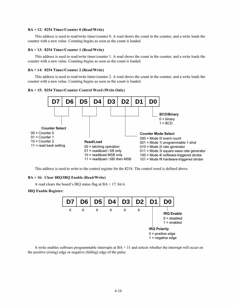
BA + 12: 8254 Timer/Counter 0 (Read/Write)
This address is used to read/write timer/counter 0. A read shows the count in the counter, and a write loads thecounter with a new value. Counting begins as soon as the count is loaded.
BA + 13: 8254 Timer/Counter 1 (Read/Write)
This address is used to read/write timer/counter 1. A read shows the count in the counter, and a write loads thecounter with a new value. Counting begins as soon as the count is loaded.
BA + 14: 8254 Timer/Counter 2 (Read/Write)
This address is used to read/write timer/counter 2. A read shows the count in the counter, and a write loads thecounter with a new value. Counting begins as soon as the count is loaded.
BA + 15: 8254 Timer/Counter Control Word (Write Only)
A write enables software programmable interrupts at BA + 31 and selects whether the interrupt will occur onthe positive (rising) edge or negative (falling) edge of the pulse.
This address is used to write to the control register for the 8254. The control word is defined above.
BA + 16: Clear IRQ/IRQ Enable (Read/Write)
A read clears the board�s IRQ status flag at BA + 17, bit 6.
IRQ Enable Register:
4-11
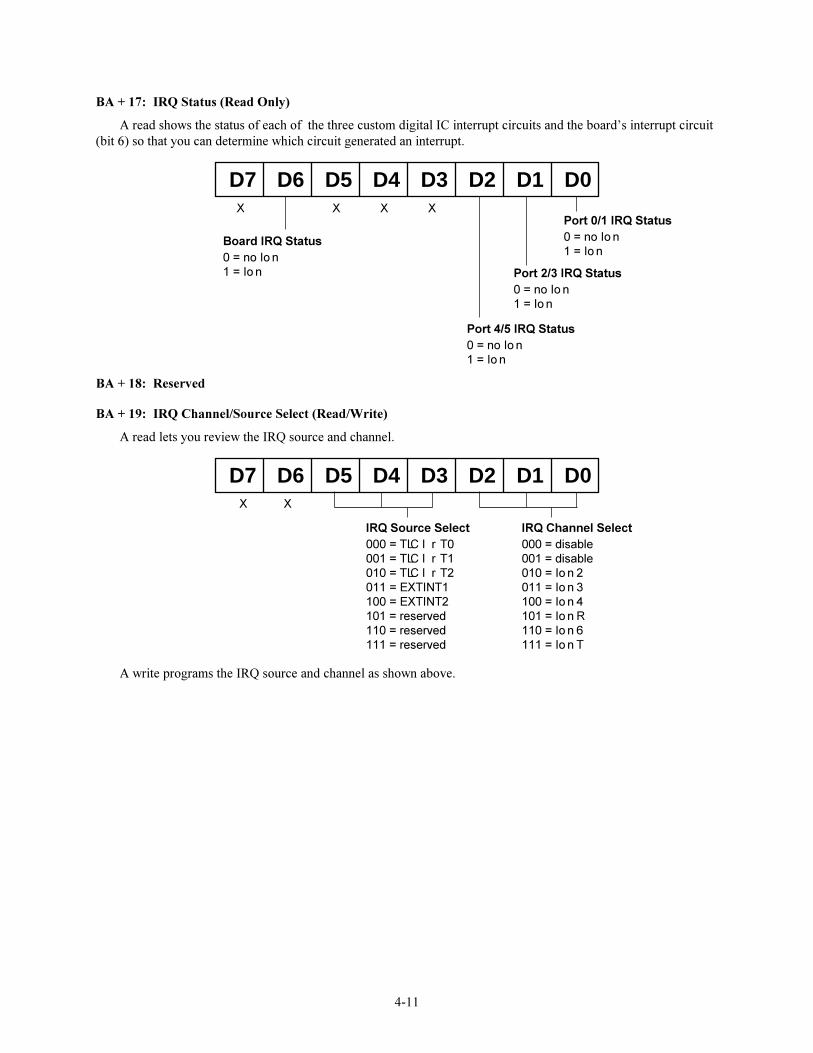
BA + 17: IRQ Status (Read Only)
A read shows the status of each of the three custom digital IC interrupt circuits and the board�s interrupt circuit(bit 6) so that you can determine which circuit generated an interrupt.
D7 D6 D5 D4 D3 D2 D1 D0
IRQ Channel Select000 = disable001 = disable010 = IRQ2011 = IRQ3100 = IRQ4101 = IRQ5110 = IRQ6111 = IRQ7
X X
IRQ Source Select000 = T/C OUT0001 = T/C OUT1010 = T/C OUT2011 = EXTINT1100 = EXTINT2101 = reserved110 = reserved111 = reserved
A write programs the IRQ source and channel as shown above.
D7 D6 D5 D4 D3 D2 D1 D0
Port 0/1 IRQ Status0 = no IRQ1 = IRQ
Port 2/3 IRQ Status0 = no IRQ1 = IRQ
Port 4/5 IRQ Status0 = no IRQ1 = IRQ
X X X X
Board IRQ Status0 = no IRQ1 = IRQ
BA + 18: Reserved
BA + 19: IRQ Channel/Source Select (Read/Write)
A read lets you review the IRQ source and channel.
4-12
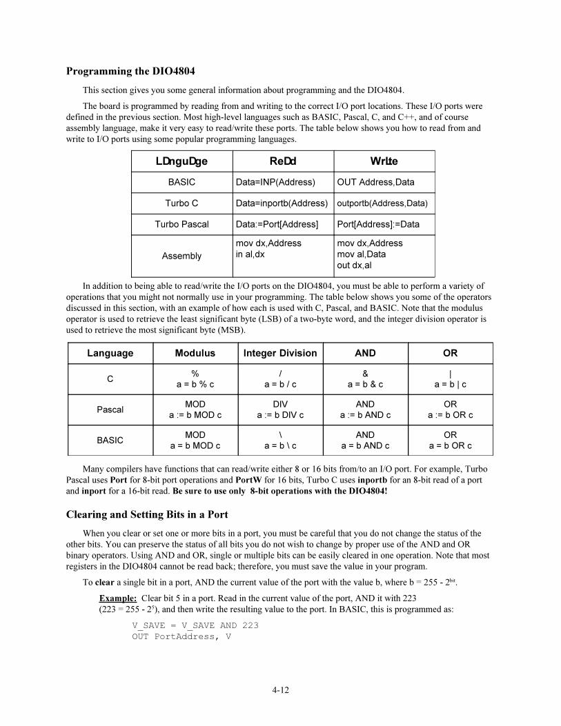
Programming the DIO4804
This section gives you some general information about programming and the DIO4804.
The board is programmed by reading from and writing to the correct I/O port locations. These I/O ports weredefined in the previous section. Most high-level languages such as BASIC, Pascal, C, and C++, and of courseassembly language, make it very easy to read/write these ports. The table below shows you how to read from andwrite to I/O ports using some popular programming languages.
In addition to being able to read/write the I/O ports on the DIO4804, you must be able to perform a variety ofoperations that you might not normally use in your programming. The table below shows you some of the operatorsdiscussed in this section, with an example of how each is used with C, Pascal, and BASIC. Note that the modulusoperator is used to retrieve the least significant byte (LSB) of a two-byte word, and the integer division operator isused to retrieve the most significant byte (MSB).
Many compilers have functions that can read/write either 8 or 16 bits from/to an I/O port. For example, TurboPascal uses Port for 8-bit port operations and PortW for 16 bits, Turbo C uses inportb for an 8-bit read of a portand inport for a 16-bit read. Be sure to use only 8-bit operations with the DIO4804!
Clearing and Setting Bits in a Port
When you clear or set one or more bits in a port, you must be careful that you do not change the status of theother bits. You can preserve the status of all bits you do not wish to change by proper use of the AND and ORbinary operators. Using AND and OR, single or multiple bits can be easily cleared in one operation. Note that mostregisters in the DIO4804 cannot be read back; therefore, you must save the value in your program.
To clear a single bit in a port, AND the current value of the port with the value b, where b = 255 - 2bit.
Example: Clear bit 5 in a port. Read in the current value of the port, AND it with 223(223 = 255 - 25), and then write the resulting value to the port. In BASIC, this is programmed as:
V_SAVE = V_SAVE AND 223OUT PortAddress, V
/ DQJXDJH 5 HDG : ULWH
%$6,& 'DWD ,13�$GGUHVV� 287�$GGUHVV�'DWD
7XUER�& 'DWD LQSRUWE�$GGUHVV� RXWSRUWE�$GGUHVV�'DWD�
7XUER�3DVFDO 'DWD� 3RUW>$GGUHVV@ 3RUW>$GGUHVV@� 'DWD
$VVHPEO\PRY�G[�$GGUHVVLQ�DO�G[
PRY�G[�$GGUHVVPRY�DO�'DWDRXW�G[�DO
/DQJXDJH 0RGXOXV ,QWHJHU�'LYLVLRQ $1' 25
&�
D� �E���F�
D� �E���F
D� �E��F_
D� �E�_�F
3DVFDO02'
D�� �E�02'�F',9
D�� �E�',9�F$1'
D�� �E�$1'�F25
D�� �E�25�F
%$6,&02'
D� �E�02'�F?
D� �E�?�F$1'
D� �E�$1'�F25
D� �E�25�F
4-13
To set a single bit in a port, OR the current value of the port with the value b, where b = 2bit.
Example: Set bit 3 in a port. Read in the current value of the port, OR it with 8 (8 = 23), and thenwrite the resulting value to the port. In Pascal, this is programmed as:
V_Save = V_Save OR 8;Port[PortAddress] := V_Save;
Setting or clearing more than one bit at a time is accomplished just as easily. To clear multiple bits in a port,AND the current value of the port with the value b, where b = 255 - (the sum of the values of the bits to be cleared).Note that the bits do not have to be consecutive.
Example: Clear bits 2, 4, and 6 in a port. Read in the current value of the port, AND it with 171(171 = 255 - 22 - 24 - 26), and then write the resulting value to the port. In C, this is programmedas:
v_save = v_save & 171;outportb(port_address, v_save);
To set multiple bits in a port, OR the current value of the port with the value b, where b = the sum of theindividual bits to be set. Note that the bits to be set do not have to be consecutive.
Example: Set bits 3, 5, and 7 in a port. Read in the current value of the port, OR it with 168(168 = 23 + 25 + 27), and then write the resulting value back to the port. In assembly language, thisis programmed as:
mov al, v_saveor al, 168mov dx, PortAddressout dx, al
Often, assigning a range of bits is a mixture of setting and clearing operations. You can set or clear each bitindividually or use a faster method of first clearing all the bits in the range then setting only those bits that must beset using the method shown above for setting multiple bits in a port. The following example shows how this two-step operation is done.
Example: Assign bits 3, 4, and 5 in a port to 101 (bits 3 and 5 set, bit 4 cleared). First, read in theport and clear bits 3, 4, and 5 by ANDing them with 199. Then set bits 3 and 5 by ORing themwith 40, and finally write the resulting value back to the port. In C, this is programmed as:
v_save = v_save & 199;v_save = v_save | 40;outportb(port_address, v_save);
A final note: Don�t be intimidated by the binary operators AND and OR and try to use operators for which youhave a better intuition. For instance, if you are tempted to use addition and subtraction to set and clear bits in placeof the methods shown above, DON�T! Addition and subtraction may seem logical, but they will not work if you tryto clear a bit that is already clear or set a bit that is already set. For example, you might think that to set bit 5 of aport, you simply need to read in the port, add 32 (25) to that value, and then write the resulting value back to the port.This works fine if bit 5 is not already set. But, what happens when bit 5 is already set? Bits 0 to 4 will be unaffectedand we can�t say for sure what happens to bits 6 and 7, but we can say for sure that bit 5 ends up cleared instead ofbeing set. A similar problem happens when you use subtraction to clear a bit in place of the method shown above.

4-14
5-1
CHAPTER 5
DIGITAL I/O
This chapter explains the bit programmable digital I/O circuitryon the DIO4804.

5-2
5-3
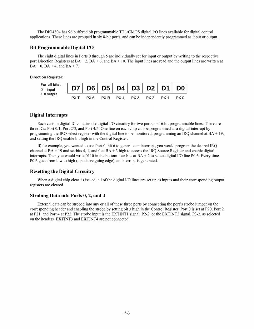
Digital Interrupts
Each custom digital IC contains the digital I/O circuitry for two ports, or 16 bit programmable lines. There arethree ICs: Port 0/1, Port 2/3, and Port 4/5. One line on each chip can be programmed as a digital interrupt byprogramming the IRQ select register with the digital line to be monitored, programming an IRQ channel at BA + 19,and setting the IRQ enable bit high in the Control Register.
If, for example, you wanted to use Port 0, bit 6 to generate an interrupt, you would program the desired IRQchannel at BA + 19 and set bits 4, 1, and 0 at BA + 3 high to access the IRQ Source Register and enable digitalinterrupts. Then you would write 0110 in the bottom four bits at BA + 2 to select digital I/O line P0.6. Every timeP0.6 goes from low to high (a positive going edge), an interrupt is generated.
Resetting the Digital Circuitry
When a digital chip clear is issued, all of the digital I/O lines are set up as inputs and their corresponding outputregisters are cleared.
Strobing Data into Ports 0, 2, and 4
External data can be strobed into any or all of these three ports by connecting the port�s strobe jumper on thecorresponding header and enabling the strobe by setting bit 3 high in the Control Register. Port 0 is set at P20, Port 2at P21, and Port 4 at P22. The strobe input is the EXTINT1 signal, P2-2, or the EXTINT2 signal, P3-2, as selectedon the headers. EXTINT3 and EXTINT4 are not connected.
The DIO4804 has 96 buffered bit programmable TTL/CMOS digital I/O lines available for digital controlapplications. These lines are grouped in six 8-bit ports, and can be independently programmed as input or output.
Bit Programmable Digital I/O
The eight digital lines in Ports 0 through 5 are individually set for input or output by writing to the respectiveport Direction Registers at BA + 2, BA + 6, and BA + 10. The input lines are read and the output lines are written atBA + 0, BA + 4, and BA + 7.
Direction Register:
D7 D6 D5 D4 D3 D2 D1 D0PX.7 PX.6 PX.5 PX.4 PX.3 PX.2 PX.1 PX.0
For all bits:0 = input1 = output

5-4
6-1
CHAPTER 6
TIMER/COUNTERS
This chapter explains the 8254 timer/counter circuit on theDIO4804.

6-2
6-3
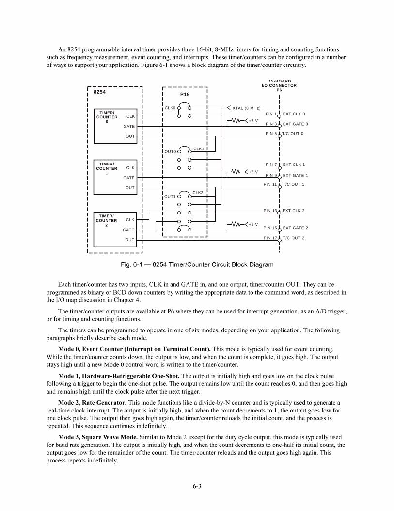
An 8254 programmable interval timer provides three 16-bit, 8-MHz timers for timing and counting functionssuch as frequency measurement, event counting, and interrupts. These timer/counters can be configured in a numberof ways to support your application. Figure 6-1 shows a block diagram of the timer/counter circuitry.
CLK1
CLK2
CLK0
ON-BOARDI/O CONNECTOR
P6
PIN 15
PIN 7
PIN 11
8254
TIMER/COUNTER
0CLK
GATE
OUT
TIMER/COUNTER
1CLK
GATE
OUT
TIMER/COUNTER
2CLK
GATE
OUT
PIN 1
PIN 17
XTAL (8 MHz)
P19
+5 V
+5 V
+5 V
PIN 3
PIN 5
PIN 9
PIN 13
T/C OUT 0
OUT0
OUT1
EXT CLK 0
T/C OUT 1
EXT CLK 1
EXT GATE 2
T/C OUT 2
EXT CLK 2
EXT GATE 0
EXT GATE 1
Fig. 6-1 � 8254 Timer/Counter Circuit Block Diagram
Each timer/counter has two inputs, CLK in and GATE in, and one output, timer/counter OUT. They can beprogrammed as binary or BCD down counters by writing the appropriate data to the command word, as described inthe I/O map discussion in Chapter 4.
The timer/counter outputs are available at P6 where they can be used for interrupt generation, as an A/D trigger,or for timing and counting functions.
The timers can be programmed to operate in one of six modes, depending on your application. The followingparagraphs briefly describe each mode.
Mode 0, Event Counter (Interrupt on Terminal Count). This mode is typically used for event counting.While the timer/counter counts down, the output is low, and when the count is complete, it goes high. The outputstays high until a new Mode 0 control word is written to the timer/counter.
Mode 1, Hardware-Retriggerable One-Shot. The output is initially high and goes low on the clock pulsefollowing a trigger to begin the one-shot pulse. The output remains low until the count reaches 0, and then goes highand remains high until the clock pulse after the next trigger.
Mode 2, Rate Generator. This mode functions like a divide-by-N counter and is typically used to generate areal-time clock interrupt. The output is initially high, and when the count decrements to 1, the output goes low forone clock pulse. The output then goes high again, the timer/counter reloads the initial count, and the process isrepeated. This sequence continues indefinitely.
Mode 3, Square Wave Mode. Similar to Mode 2 except for the duty cycle output, this mode is typically usedfor baud rate generation. The output is initially high, and when the count decrements to one-half its initial count, theoutput goes low for the remainder of the count. The timer/counter reloads and the output goes high again. Thisprocess repeats indefinitely.

6-4
Mode 4, Software-Triggered Strobe. The output is initially high. When the initial count expires, the outputgoes low for one clock pulse and then goes high again. Counting is �triggered� by writing the initial count.
Mode 5, Hardware Triggered Strobe (Retriggerable). The output is initially high. Counting is triggered bythe rising edge of the gate input. When the initial count has expired, the output goes low for one clock pulse andthen goes high again.
Appendix C provides the 8254 data sheet.
7-1
CHAPTER 7
INTERRUPTS
This chapter explains programmable interrupts, digital inter-rupts, and basic interrupt programming techniques.

7-2
7-3
The DIO4804 has four interrupt circuits which can generate interrupts on any IRQ channel 2 through 7.
Software Programmable Interrupts
The DIO4804 circuitry has five software selectable interrupt sources which can be selected at BA + 19, bits 3through 5, as described in Chapter 4.
To use these interrupts, an interrupt source must be selected at BA + 19, an interrupt channel must be enabled atBA + 19, bits 0 through 2, and the IRQ enable must be set high (BA + 16, bit 0). BA + 16, bit 1 sets the polarity ofthe interrupt.
Digital Interrupts
Each custom digital IC (Port 0/1, Port 2/3, and Port 4/5) supports a digital interrupt using one of the digital I/Olines as the interrupt source. The interrupt source is software programmable as described in Chapter 5.
Sampling Digital Lines for Change of State
In the Digital Interrupt mode, the digital lines are sampled at a rate set by the 8 MHz system clock or the clockprogrammed in the timer/counter programmed at bit 5 of the port�s Digital Mode Register. With each clock pulse,the digital circuitry looks at the state of the next bit. To provide noise rejection and prevent erroneous interruptgeneration because of noise spikes on the digital lines, a change in the state of any bit must be seen for two edges ofa clock pulse to be recognized by the circuit. Figure 7-1 shows a diagram of this circuit.
Selecting the Interrupt Channel
The IRQ channel is selected by programming the IRQ channel at BA + 19, bits 0 through 2.
To determine which interrupt source has generated an interrupt, you must check bits 0 through 2 of the statusword read at BA + 17. Then service the interrupt that has occurred and clear the interrupt (the software program-mable interrupt is cleared by reading BA + 16, and the digital interrupts are cleared by setting bits 1 and 0 in thecorresponding port�s Control Register and performing a read at the Port Direction/IRQ Source Register address).
Fig. 7-1 � Digital Interrupt Timing Diagram
DIGITAL INPUT
CLOCK
IRQ OUT
7-4
Basic Programming For Interrupt Handling
What Is an Interrupt?
An interrupt is an event that causes the processor in your computer to temporarily halt its current process andexecute another routine. Upon completion of the new routine, control is returned to the original routine at the pointwhere its execution was interrupted.
Interrupts are very handy for dealing with asynchronous events (events that occur at less than regular intervals).Keyboard activity is a good example; your computer cannot predict when you might press a key and it would be awaste of processor time for it to do nothing while waiting for a keystroke to occur. Thus, the interrupt scheme isused and the processor proceeds with other tasks. Then, when a keystroke does occur, the keyboard �interrupts� theprocessor, and the processor gets the keyboard data, places it in memory, and then returns to what it was doingbefore it was interrupted. Other common devices that use interrupts are modems, disk drives, and mice.
Your DIO4804 can interrupt the processor when a variety of conditions are met. By using these interrupts, youcan write software that effectively deals with real world events.
Interrupt Request Lines
To allow different peripheral devices to generate interrupts on the same computer, the PC bus has eight differentinterrupt request (IRQ) lines. A transition from low to high on one of these lines generates an interrupt requestwhich is handled by the PC�s interrupt controller. The interrupt controller checks to see if interrupts are to beacknowledged from that IRQ and, if another interrupt is already in progress, it decides if the new request shouldsupersede the one in progress or if it has to wait until the one in progress is done. This prioritizing allows aninterrupt to be interrupted if the second request has a higher priority. The priority level is based on the number of theIRQ; IRQ0 has the highest priority, IRQ1 is second-highest, and so on through IRQ7, which has the lowest. Many ofthe IRQs are used by the standard system resources. IRQ0 is used by the system timer, IRQ1 is used by the key-board, IRQ3 by COM2, IRQ4 by COM1, and IRQ6 by the disk drives. Therefore, it is important for you to knowwhich IRQ lines are available in your system for use by the board.
8259 Programmable Interrupt Controller
The chip responsible for handling interrupt requests in the PC is the 8259 Programmable Interrupt Controller.To use interrupts, you need to know how to read and set the 8259�s interrupt mask register (IMR) and how to sendthe end-of-interrupt (EOI) command to the 8259.
- Interrupt Mask Register (IMR)
Each bit in the interrupt mask register (IMR) contains the mask status of an IRQ line; bit 0 is for IRQ0, bit 1 isfor IRQ1, and so on. If a bit is set (equal to 1), then the corresponding IRQ is masked and it will not generate aninterrupt. If a bit is clear (equal to 0), then the corresponding IRQ is unmasked and can generate interrupts. TheIMR is programmed through port 21H.
- End-of-Interrupt (EOI) Command
After an interrupt service routine is complete, the 8259 interrupt controller must be notified. This is done bywriting the value 20H to I/O port 20H.
For all bits:0 = IRQ unmasked (enabled)1 = IRQ masked (disabled)
I/O Port 21H,54� ,54� ,54� ,54� ,54� ,54� ,54� ,54�
7-5
What Exactly Happens When an Interrupt Occurs?
Understanding the sequence of events when an interrupt is triggered is necessary to properly write softwareinterrupt handlers. When an interrupt request line is driven high by a peripheral device (such as the DIO9604), theinterrupt controller checks to see if interrupts are enabled for that IRQ, and then checks to see if other interrupts areactive or requested and determines which interrupt has priority. The interrupt controller then interrupts the proces-sor. The current code segment (CS), instruction pointer (IP), and flags are pushed on the stack for storage, and a newCS and IP are loaded from a table that exists in the lowest 1024 bytes of memory. This table is referred to as theinterrupt vector table and each entry is called an interrupt vector. Once the new CS and IP are loaded from theinterrupt vector table, the processor begins executing the code located at CS:IP. When the interrupt routine iscompleted, the CS, IP, and flags that were pushed on the stack when the interrupt occurred are now popped from thestack and execution resumes from the point where it was interrupted.
Using Interrupts in Your Programs
Adding interrupts to your software is not as difficult as it may seem, and what they add in terms of performanceis often worth the effort. Note, however, that although it is not that hard to use interrupts, the smallest mistake willoften lead to a system hang that requires a reboot. This can be both frustrating and time-consuming. But, after a fewtries, you�ll get the bugs worked out and enjoy the benefits of properly executed interrupts. In addition to reading thefollowing paragraphs, study the INTRPTS source code included on your DIO4804 program disk for a betterunderstanding of interrupt program development.
Writing an Interrupt Service Routine (ISR)
The first step in adding interrupts to your software is to write the interrupt service routine (ISR). This is theroutine that will automatically be executed each time an interrupt request occurs on the specified IRQ. An ISR isdifferent than standard routines that you write. First, on entrance, the processor registers should be pushed onto thestack BEFORE you do anything else. Second, just before exiting your ISR, you must clear the interrupt status flagof the DIO4804 and write an end-of-interrupt command to the 8259 controller. Finally, when exiting the ISR, inaddition to popping all the registers you pushed on entrance, you must use the IRET instruction and not a plainRET. The IRET automatically pops the flags, CS, and IP that were pushed when the interrupt was called.
If you find yourself intimidated by interrupt programming, take heart. Most Pascal and C compilers allow youto identify a procedure (function) as an interrupt type and will automatically add these instructions to your ISR, withone important exception: most compilers do not automatically add the end-of-interrupt command to the procedure;you must do this yourself. Other than this and the few exceptions discussed below, you can write your ISR just likeany other routine. It can call other functions and procedures in your program and it can access global data. If you arewriting your first ISR, we recommend that you stick to the basics; just something that will convince you that itworks, such as incrementing a global variable.
NOTE: If you are writing an ISR using assembly language, you are responsible for pushing and poppingregisters and using IRET instead of RET.
There are a few cautions you must consider when writing your ISR. The most important is, do not use anyDOS functions or routines that call DOS functions from within an ISR. DOS is not reentrant; that is, a DOSfunction cannot call itself. In typical programming, this will not happen because of the way DOS is written. Butwhat about when using interrupts? Then, you could have a situation such as this in your program. If DOS function Xis being executed when an interrupt occurs and the interrupt routine makes a call to DOS function X, then functionX is essentially being called while it is already active. Such a reentrancy attempt spells disaster because DOSfunctions are not written to support it. This is a complex concept and you do not need to understand it. Just makesure that you do not call any DOS functions from within your ISR. The one wrinkle is that, unfortunately, it is notobvious which library routines included with your compiler use DOS functions. A rule of thumb is that routineswhich write to the screen, or check the status of or read the keyboard, and any disk I/O routines use DOS and shouldbe avoided in your ISR.
The same problem of reentrancy exists for many floating point emulators as well, meaning you may have toavoid floating point (real) math in your ISR.
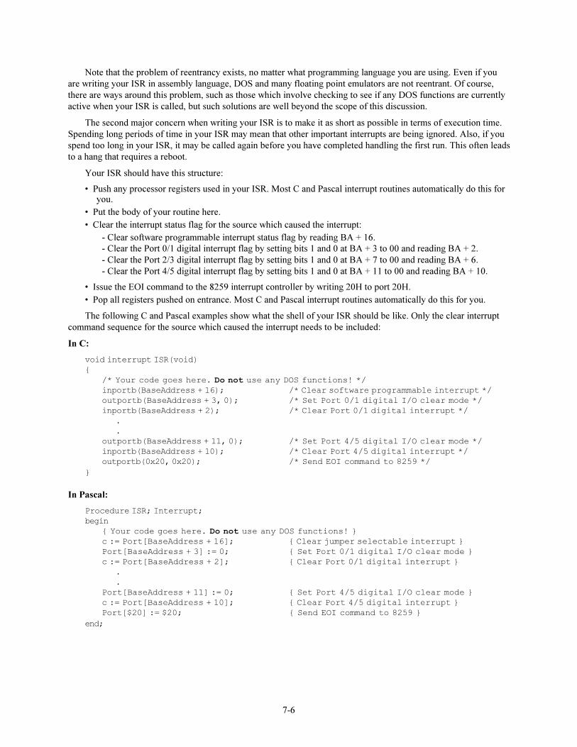
7-6
Note that the problem of reentrancy exists, no matter what programming language you are using. Even if youare writing your ISR in assembly language, DOS and many floating point emulators are not reentrant. Of course,there are ways around this problem, such as those which involve checking to see if any DOS functions are currentlyactive when your ISR is called, but such solutions are well beyond the scope of this discussion.
The second major concern when writing your ISR is to make it as short as possible in terms of execution time.Spending long periods of time in your ISR may mean that other important interrupts are being ignored. Also, if youspend too long in your ISR, it may be called again before you have completed handling the first run. This often leadsto a hang that requires a reboot.
Your ISR should have this structure:
� Push any processor registers used in your ISR. Most C and Pascal interrupt routines automatically do this foryou.
� Put the body of your routine here.� Clear the interrupt status flag for the source which caused the interrupt:
- Clear software programmable interrupt status flag by reading BA + 16.- Clear the Port 0/1 digital interrupt flag by setting bits 1 and 0 at BA + 3 to 00 and reading BA + 2.- Clear the Port 2/3 digital interrupt flag by setting bits 1 and 0 at BA + 7 to 00 and reading BA + 6.- Clear the Port 4/5 digital interrupt flag by setting bits 1 and 0 at BA + 11 to 00 and reading BA + 10.
� Issue the EOI command to the 8259 interrupt controller by writing 20H to port 20H.� Pop all registers pushed on entrance. Most C and Pascal interrupt routines automatically do this for you.
The following C and Pascal examples show what the shell of your ISR should be like. Only the clear interruptcommand sequence for the source which caused the interrupt needs to be included:
In C:
void interrupt ISR(void){
/* Your code goes here. Do not use any DOS functions! */inportb(BaseAddress + 16); /* Clear software programmable interrupt */outportb(BaseAddress + 3, 0); /* Set Port 0/1 digital I/O clear mode */inportb(BaseAddress + 2); /* Clear Port 0/1 digital interrupt */ . .outportb(BaseAddress + 11, 0); /* Set Port 4/5 digital I/O clear mode */inportb(BaseAddress + 10); /* Clear Port 4/5 digital interrupt */outportb(0x20, 0x20); /* Send EOI command to 8259 */
}
In Pascal:
Procedure ISR; Interrupt;begin
{ Your code goes here. Do not use any DOS functions! }c := Port[BaseAddress + 16]; { Clear jumper selectable interrupt }Port[BaseAddress + 3] := 0; { Set Port 0/1 digital I/O clear mode }c := Port[BaseAddress + 2]; { Clear Port 0/1 digital interrupt } . .Port[BaseAddress + 11] := 0; { Set Port 4/5 digital I/O clear mode }c := Port[BaseAddress + 10]; { Clear Port 4/5 digital interrupt }Port[$20] := $20; { Send EOI command to 8259 }
end;
7-7
Saving the Startup Interrupt Mask Register (IMR) and Interrupt Vector
The next step after writing the ISR is to save the startup state of the interrupt mask register and the interruptvector that you will be using. The IMR is located at I/O port 21H. The interrupt vector you will be using is locatedin the interrupt vector table which is simply an array of 256-bit (4-byte) pointers and is located in the first 1024bytes of memory (Segment = 0, Offset = 0). You can read this value directly, but it is a better practice to use DOSfunction 35H (get interrupt vector). Most C and Pascal compilers provide a library routine for reading the value of avector. The vectors for the hardware interrupts are vectors 8 through 15, where IRQ0 uses vector 8, IRQ1 usesvector 9, and so on. Thus, if the DIO4804 will be using IRQ3, you should save the value of interrupt vector 11.
Before you install your ISR, temporarily mask out the IRQ you will be using. This prevents the IRQ fromrequesting an interrupt while you are installing and initializing your ISR. To mask the IRQ, read in the current IMRat I/O port 21H and set the bit that corresponds to your IRQ (remember, setting a bit disables interrupts on that IRQwhile clearing a bit enables them). The IMR is arranged so that bit 0 is for IRQ0, bit 1 is for IRQ1, and so on. Seethe paragraph entitled Interrupt Mask Register (IMR) earlier in this chapter for help in determining your IRQ�s bit.After setting the bit, write the new value to I/O port 21H.
With the startup IMR saved and the interrupts on your IRQ temporarily disabled, you can assign the interruptvector to point to your ISR. Again, you can overwrite the appropriate entry in the vector table with a direct memorywrite, but this is a bad practice. Instead, use either DOS function 25H (set interrupt vector) or, if your compilerprovides it, the library routine for setting an interrupt vector. Remember that vector 8 is for IRQ0, vector 9 is forIRQ1, and so on.
If you need to program the source of your interrupts, do that next. For example, if you are using the program-mable interval timer to generate interrupts, you must program it to run in the proper mode and at the proper rate.
Finally, clear the bit in the IMR for the IRQ you are using. This enables interrupts on the IRQ.
Restoring the Startup IMR and Interrupt Vector
Before exiting your program, you must restore the interrupt mask register and interrupt vectors to the state theywere in when your program started. To restore the IMR, write the value that was saved when your program startedto I/O port 21H. Restore the interrupt vector that was saved at startup with either DOS function 35H (get interruptvector), or use the library routine supplied with your compiler. Performing these two steps will guarantee that theinterrupt status of your computer is the same after running your program as it was before your program startedrunning.
Common Interrupt Mistakes
� Remember that hardware interrupts are numbered 8 through 15, even though the corresponding IRQs arenumbered 0 through 7.
� Two of the most common mistakes when writing an ISR are forgetting to clear the interrupt status of theDIO4804 and forgetting to issue the EOI command to the 8259 interrupt controller before exiting the ISR.

7-8

A-1
APPENDIX A
DIO4804 SPECIFICATIONS

A-2
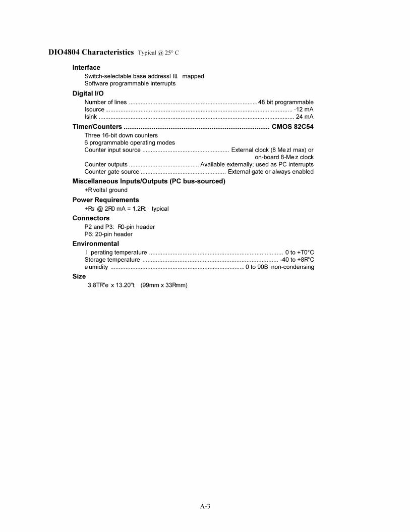
A-3
DIO4804 Characteristics Typical @ 25° C
InterfaceSwitch-selectable base address, I/O mappedSoftware programmable interrupts
Digital I/ONumber of lines .............................................................................48 bit programmableIsource ................................................................................................................ -12 mAIsink ..................................................................................................................... 24 mA
Timer/Counters .............................................................................. CMOS 82C54Three 16-bit down counters6 programmable operating modesCounter input source .................................................... External clock (8 MHz, max) or
on-board 8-MHz clockCounter outputs .......................................... Available externally; used as PC interruptsCounter gate source ................................................... External gate or always enabled
Miscellaneous Inputs/Outputs (PC bus-sourced)+5 volts, ground
Power Requirements+5V @ 250 mA = 1.25W typical
ConnectorsP2 and P3: 50-pin headerP6: 20-pin header
Environmental Operating temperature ................................................................................ 0 to +70°CStorage temperature ................................................................................. -40 to +85°CHumidity ................................................................................ 0 to 90% non-condensing
Size 3.875"H x 13.20"W (99mm x 335mm)

A-4

B-1
APPENDIX B
CONNECTOR PIN ASSIGNMENTS

B-2
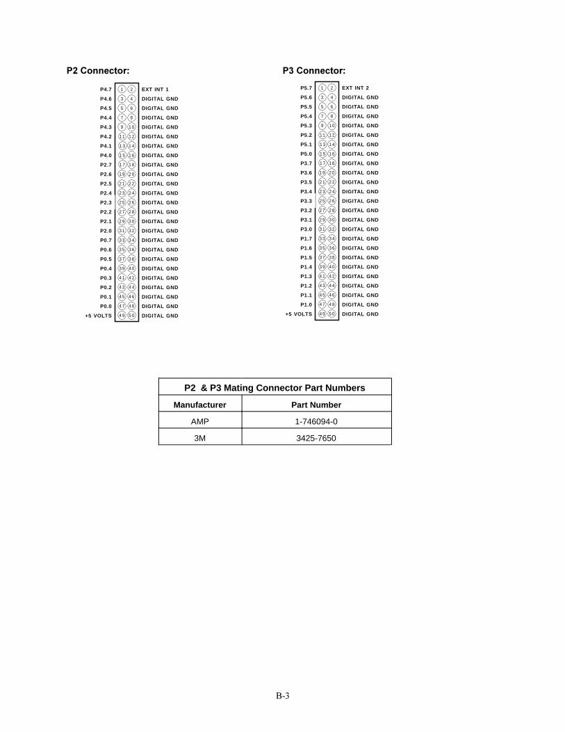
B-3
P2 Connector:
3 9 4 0
3 7 3 8
3 5 3 6
3 3 3 4
3 1 3 2
2 9 3 0
2 7 2 8
2 5 2 6
2 3 2 4
2 1 2 2
1 9 2 0
1 7 1 8
1 5 1 6
1 3 1 4
11 1 2
9 1 0
7 8
5 6
3 4
1 2
4 9 5 0
4 7 4 8
4 5 4 6
4 3 4 4
4 1 4 2
P4.7
P4.6
P4.5
P4.4
P4.3
P4.2
P4.1
P4.0
P2.7
P2.6
P2.5
P2.4
P2.3
P2.2
P2.1
P2.0
P0.7
P0.6
P0.5
P0.4
P0.3
P0.2
P0.1
P0.0
+5 VOLTS
EXT INT 1
DIGITAL GND
DIGITAL GND
DIGITAL GND
DIGITAL GND
DIGITAL GND
DIGITAL GND
DIGITAL GND
DIGITAL GND
DIGITAL GND
DIGITAL GND
DIGITAL GND
DIGITAL GND
DIGITAL GND
DIGITAL GND
DIGITAL GND
DIGITAL GND
DIGITAL GND
DIGITAL GND
DIGITAL GND
DIGITAL GND
DIGITAL GND
DIGITAL GND
DIGITAL GND
DIGITAL GND
3 9 4 0
3 7 3 8
3 5 3 6
3 3 3 4
3 1 3 2
2 9 3 0
2 7 2 8
2 5 2 6
2 3 2 4
2 1 2 2
1 9 2 0
1 7 1 8
1 5 1 6
1 3 1 4
11 1 2
9 1 0
7 8
5 6
3 4
1 2
4 9 5 0
4 7 4 8
4 5 4 6
4 3 4 4
4 1 4 2
P5.7
P5.6
P5.5
P5.4
P5.3
P5.2
P5.1
P5.0
P3.7
P3.6
P3.5
P3.4
P3.3
P3.2
P3.1
P3.0
P1.7
P1.6
P1.5
P1.4
P1.3
P1.2
P1.1
P1.0
+5 VOLTS
EXT INT 2
DIGITAL GND
DIGITAL GND
DIGITAL GND
DIGITAL GND
DIGITAL GND
DIGITAL GND
DIGITAL GND
DIGITAL GND
DIGITAL GND
DIGITAL GND
DIGITAL GND
DIGITAL GND
DIGITAL GND
DIGITAL GND
DIGITAL GND
DIGITAL GND
DIGITAL GND
DIGITAL GND
DIGITAL GND
DIGITAL GND
DIGITAL GND
DIGITAL GND
DIGITAL GND
DIGITAL GND
P3 Connector:
P2 & P3 Mating Connector Part Numbers
Manufacturer Part Number
AMP 1-746094-0
3M 3425-7650
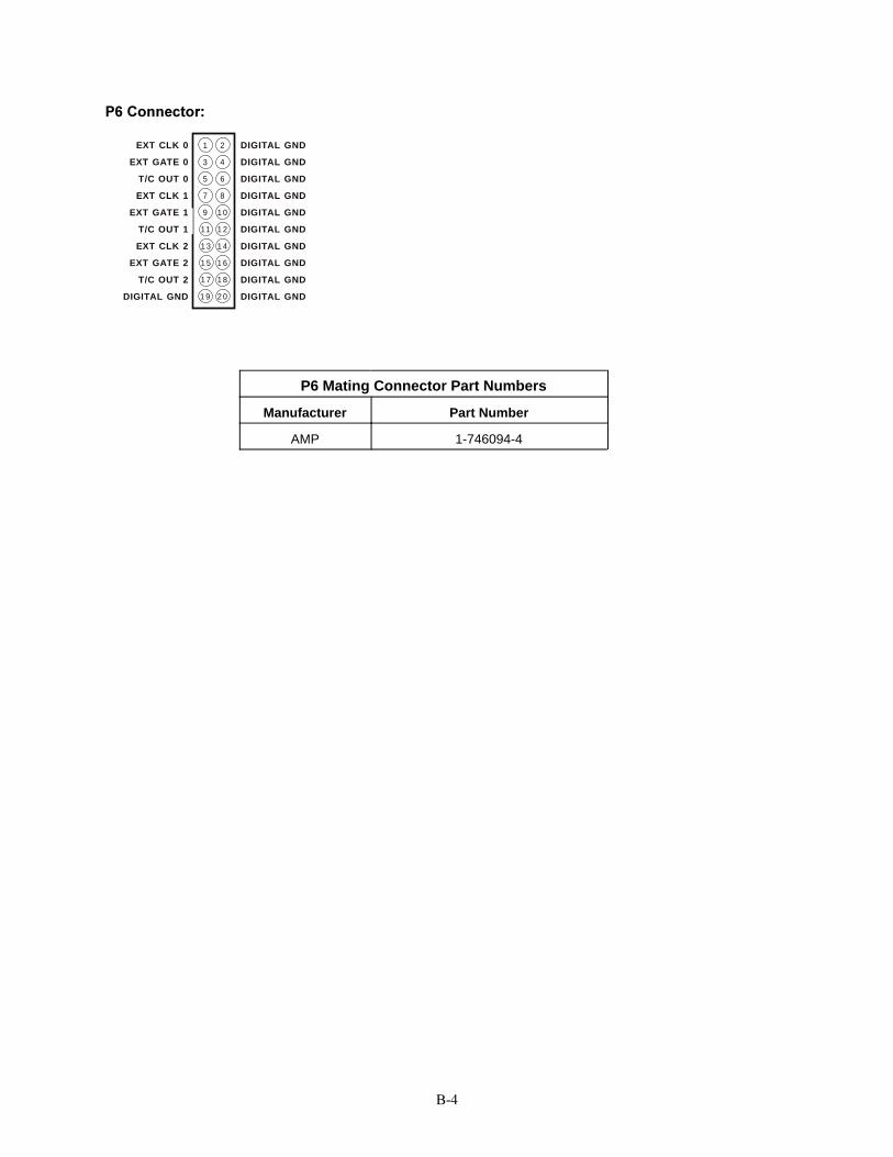
B-4
P6 Connector:
1 9 2 0
1 7 1 8
1 5 1 6
1 3 1 4
11 1 2
9 1 0
7 8
5 6
3 4
1 2EXT CLK 0
EXT GATE 0
T/C OUT 0
EXT CLK 1
EXT GATE 1
T/C OUT 1
EXT CLK 2
EXT GATE 2
T/C OUT 2
DIGITAL GND
DIGITAL GND
DIGITAL GND
DIGITAL GND
DIGITAL GND
DIGITAL GND
DIGITAL GND
DIGITAL GND
DIGITAL GND
DIGITAL GND
DIGITAL GND
P6 Mating Connector Part Numbers
Manufacturer Part Number
AMP 1-746094-4

C-1
APPENDIX C
COMPONENT DATA SHEETS


Intel 82C54 Programmable Interval TimerData Sheet Reprint


D-1
APPENDIX D
WARRANTY

D-2

D-3
LIMITED WARRANTY
Real Time Devices, Inc. warrants the hardware and software products it manufactures and produces to be freefrom defects in materials and workmanship for one year following the date of shipment from REAL TIME DE-VICES. This warranty is limited to the original purchaser of product and is not transferable.
During the one year warranty period, REAL TIME DEVICES will repair or replace, at its option, any defectiveproducts or parts at no additional charge, provided that the product is returned, shipping prepaid, to REAL TIMEDEVICES. All replaced parts and products become the property of REAL TIME DEVICES. Before returning anyproduct for repair, customers are required to contact the factory for an RMA number.
THIS LIMITED WARRANTY DOES NOT EXTEND TO ANY PRODUCTS WHICH HAVE BEEN DAM-AGED AS A RESULT OF ACCIDENT, MISUSE, ABUSE (such as: use of incorrect input voltages, improper orinsufficient ventilation, failure to follow the operating instructions that are provided by REAL TIME DEVICES,�acts of God� or other contingencies beyond the control of REAL TIME DEVICES), OR AS A RESULT OFSERVICE OR MODIFICATION BY ANYONE OTHER THAN REAL TIME DEVICES. EXCEPT AS EX-PRESSLY SET FORTH ABOVE, NO OTHER WARRANTIES ARE EXPRESSED OR IMPLIED, INCLUDING,BUT NOT LIMITED TO, ANY IMPLIED WARRANTIES OF MERCHANTABILITY AND FITNESS FOR APARTICULAR PURPOSE, AND REAL TIME DEVICES EXPRESSLY DISCLAIMS ALL WARRANTIES NOTSTATED HEREIN. ALL IMPLIED WARRANTIES, INCLUDING IMPLIED WARRANTIES FORMECHANTABILITY AND FITNESS FOR A PARTICULAR PURPOSE, ARE LIMITED TO THE DURATIONOF THIS WARRANTY. IN THE EVENT THE PRODUCT IS NOT FREE FROM DEFECTS AS WARRANTEDABOVE, THE PURCHASER�S SOLE REMEDY SHALL BE REPAIR OR REPLACEMENT AS PROVIDEDABOVE. UNDER NO CIRCUMSTANCES WILL REAL TIME DEVICES BE LIABLE TO THE PURCHASEROR ANY USER FOR ANY DAMAGES, INCLUDING ANY INCIDENTAL OR CONSEQUENTIAL DAM-AGES, EXPENSES, LOST PROFITS, LOST SAVINGS, OR OTHER DAMAGES ARISING OUT OF THE USEOR INABILITY TO USE THE PRODUCT.
SOME STATES DO NOT ALLOW THE EXCLUSION OR LIMITATION OF INCIDENTAL OR CONSE-QUENTIAL DAMAGES FOR CONSUMER PRODUCTS, AND SOME STATES DO NOT ALLOW LIMITA-TIONS ON HOW LONG AN IMPLIED WARRANTY LASTS, SO THE ABOVE LIMITATIONS OR EXCLU-SIONS MAY NOT APPLY TO YOU.
THIS WARRANTY GIVES YOU SPECIFIC LEGAL RIGHTS, AND YOU MAY ALSO HAVE OTHERRIGHTS WHICH VARY FROM STATE TO STATE.

DIO4804 User Settings
Base I/O Address:
(hex) (decimal)


