Lehrstuhl für Hochfrequenztechnik der Technischen Universität München Univ.-Prof. Dr. techn. Peter Russer A Si Schottky Diode Demultiplexer Circuit for High Bit Rate Fiber Optical Receivers Jung Han Choi Vollständiger Abdruck der von der Fakultät für Elektrotechnik und Informationstechnik der Technischen Universtät München zur Erlangung des akademischen Grades eines Doktor-Ingenieurs genehmigten Dissertation. Vorsitzender: Univ.-Prof. Dr.-Ing. Fernando Puente León Prüfer der Dissertation: 1. Univ.-Prof. Dr. techn. Peter Russer 2. Univ.-Prof. Dr.-Ing. Norbert Hanik Die Dissertation wurde am 15.06.2004 bei der Technischen Universität München eingereicht und durch die Fakultät für Elektrotechnik und Informationstechnik am 31.08.2004 angenommen.
Transcript
Lehrstuhl für Hochfrequenztechnik der Technischen Universität München
Univ.-Prof. Dr. techn. Peter Russer
A Si Schottky Diode Demultiplexer Circuit
for High Bit Rate Fiber Optical Receivers
Jung Han Choi
Vollständiger Abdruck der von der Fakultät für Elektrotechnik und Informationstechnik der
Technischen Universtät München zur Erlangung des akademischen Grades eines
Doktor-Ingenieurs
genehmigten Dissertation.
Vorsitzender: Univ.-Prof. Dr.-Ing. Fernando Puente León
Prüfer der Dissertation: 1. Univ.-Prof. Dr. techn. Peter Russer
2. Univ.-Prof. Dr.-Ing. Norbert Hanik
Die Dissertation wurde am 15.06.2004 bei der Technischen Universität München eingereicht
und durch die Fakultät für Elektrotechnik und Informationstechnik am 31.08.2004
angenommen.
i
Abstract
A novel demultiplexer circuit for high bit rate fiber optic receiver applications using Si
Schottky diodes has been developed and investigated experimentally. A sampling circuit
based demultiplexer circuit theory is presented and simulated for a direct detection optical
receiver with optical preamplification. For the experimental demonstration of the
demultiplexer, very high-speed Si Schottky diodes are modeled applying the Root-diode
model. The diode parameters were obtained using a parameter extraction software, and
compared with the measurement data for various bias conditions until 40 GHz. The flip-chip
bonding connections were simulated with a three dimensional electro-magnetic simulator, and
an equivalent circuit model was established and used for the simulation of the complete
demultiplexer circuit. The Root-diode model including the flip-chip equivalent circuits
showed a good agreement with the measurement data up to 50 GHz. The hybrid technology
using alumina substrates ( Al2O3 ) of 250 µm thickness was used for the implementation.
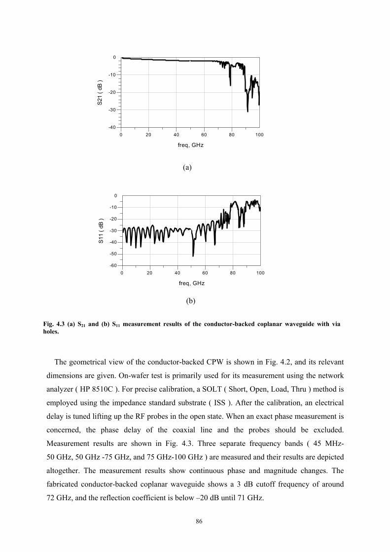
Conductor-backed coplanar waveguides were designed, fabricated and characterized by
measurements. A 3 dB cutoff frequency of 72 GHz, and a reflection coefficient ( S11 ) of
–20 dB until 70 GHz were obtained.
Using the extracted diode model and the developed flip-chip bonding equivalent circuit, the
diode sampling circuit was designed and simulated. For the purpose of reducing deterministic
intersymbol interferences, an equalizer circuit with zero-forcing algorithm was designed and
simulated. The simulation results showed an enhanced eye diagram. The designed sampling
circuit was fabricated, and measured using a 43 Gbit/s pseudo random binary sequence
( PRBS ) input signal. The measurement results displayed the demultiplexed signal output, as
expected in the simulation.
The advantage of the demultiplexer concept described in this work is that it does not
require high-speed active three-terminal devices ( e.g. HBTs, HEMTs ). The complete
demultiplexer circuit is based on Schottky diodes only. The only active circuit required in this
concept is the clock oscillator which needs to provide a clock signal at half the bit rate. If the
clock oscillator is realized as a push-push oscillator [13], the transistors need to generate
oscillation at a frequency corresponding to only a quarter of the bit rate. Therefore this
concept opens the door for future Si-based monolithically integrated demultiplexer for bit
rates up to 160 Gbit/s. Using the matured Si technology, the high-speed digital circuit can be
constructed by an analog circuit using two-terminal devices, namely Si Schottky diodes. This
ii
method is expected to reduce the bottleneck in the electronic part of optical communication
links. Many issues during circuit design and test, such as power consumption, yield, and
reliability, can be solved and never-reached high-speed circuits might be implemented in this
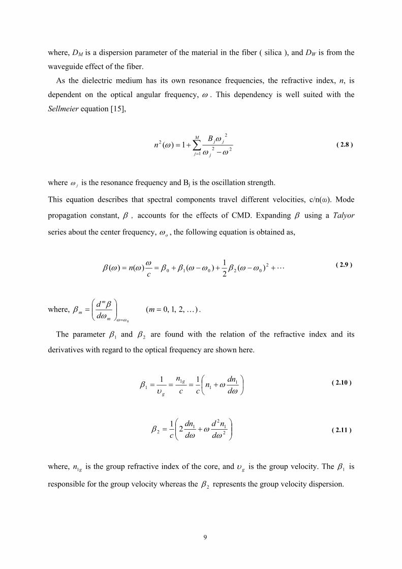
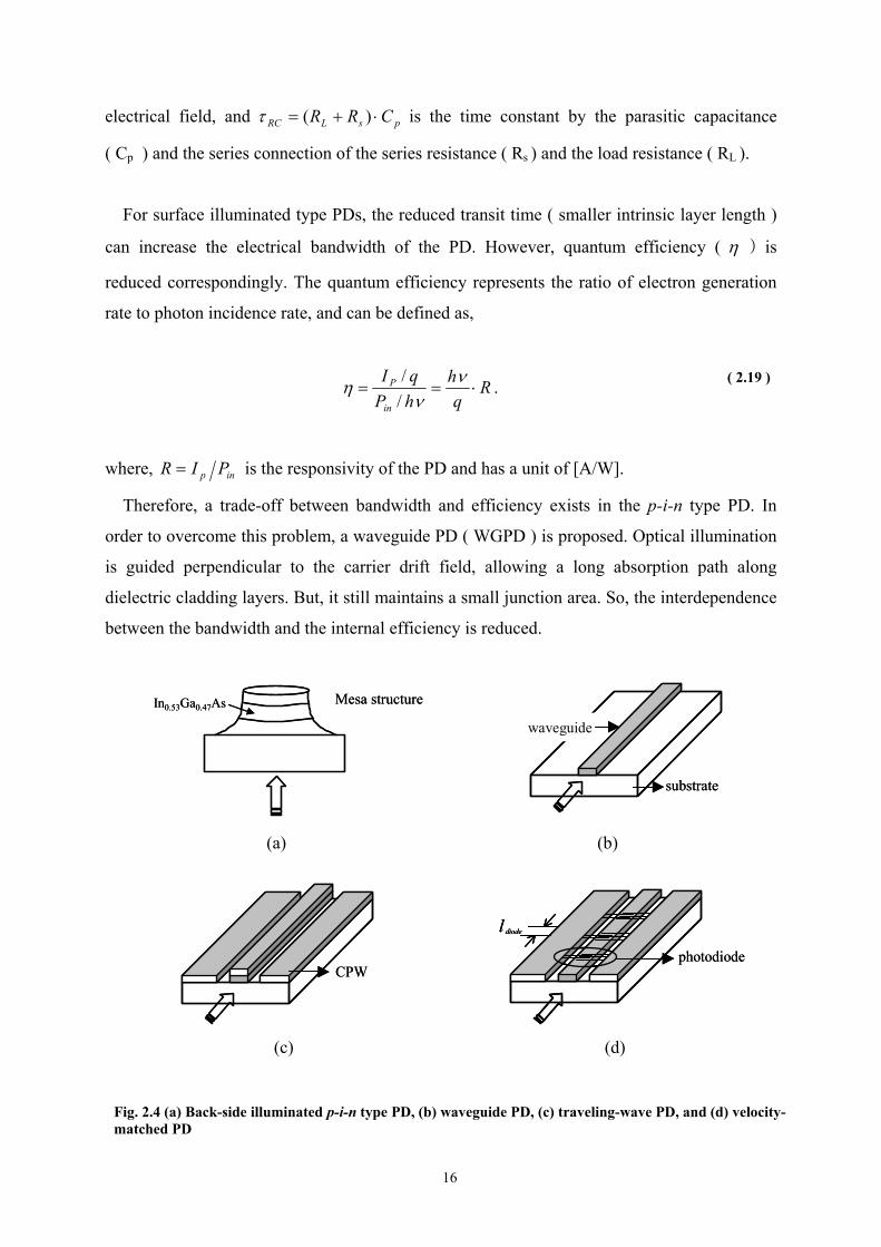
where, α is an absorption constant, Γ is a confinement factor of the light, and L is the whole
optical dielectric waveguide. In general, the optical light confinement factor is given using the
optical field distribution at the PD.
∫
∫∞
∞−
=Γdyy
dyy
yj
layerabsorption
yj
2
2
)(
)(
φ
φ
where, )(yyjφ is the optical field in the waveguide, and y is the direction perpendicular to the
diode junction layer. Physically, the confinement factor describes how much the incident
optical power effectively couples to the absorption layer. In practice, the optical field at the
WGPD is much narrower than the transverse extension of the optical field from the fiber. In
[23], a multimode WGPD is proposed enlarging the optical field at the PD without sacrificing
the bandwidth. High-doped quaternary InGaAsP forms double core around InGaAs
absorption layer and confines the optical field in transverse direction. Thus, the increased
coupling efficiency was obtained successively.
There is an inherent defect in the WGPD that the electrical signal is reflected if the
electrical waveguide is not terminated correctly. This causes pulse broadening. Matching the
characteristic impedance of the PD and supporting coplanar waveguide along the dielectric
waveguide, a traveling-wave photodetector ( TWPD ) is designed and implemented [24]. The
dBf3 in the TWPD can be expressed below
23
1
+
=
VM
t
tdB
ff
ff
( 2.20 )
( 2.21 )
( 2.22 )
18
where, tf is an electrical bandwidth limited by the carrier transit time, and VMf is defined for
matched termination at the output using electrical wave velocity ( eυ ) and optical wave
velocity ( oυ ) in the semiconductor [22] as below,
−
Γ=
o
e
eVMf
υυ
π
αυ
12
Velocity mismatch occurs because the electrical signal along the coplanar waveguide
( CPW ) travels in different velocity with the guided optical signal along the waveguide. As
eυ is given,
00
1wZ
dCL rtrtr
e εευ =
⋅=
where, d is the transit layer thickness, w is the width of the WGPD, and Z0 is characteristic
impedance of the CPW ( trtr CL= ), the electrical velocity can be as close as to the optical
light velocity in the waveguide choosing the proper CPW geometry parameters. The quantum
efficiency of the TWPD ( input matching case ) is expressed by
21 L
TWPDe Γ−−
=α
η .
Considering the high power capability of the PD, we should consider saturation current in
each type PD. For the TWPD [21],
∫=
Γ−
Γ=Γ⋅
Γ⋅=
L
xTWPDs
xTWPDSAT IWdxePdWqI
00, 2
1 ηα
α α
where, sI is the saturation photocurrent density per unit area, and oP is the incident photon
flux per unit area at the saturation condition ( sec//1 2mµ ). In the same way, for the WGPD
[21],
( 2.23 )
( 2.24 )
( 2.25 )
( 2.26 )
19
WGPDsWGPDSAT IWI ηα Γ
=,
As Γα decreases, TWPDSATI , value increases, which provides improved power handing
capability. In contrast to the increased TWPDSATI , , the 3dB bandwidth decreases as the VMf is
proportional to Γα . Therefore, there exists a trade-off between the bandwidth and the power
capability in the TWPD.
The velocity mismatch can be eliminated by periodic capacitance loading effect. In fact, the
electrical signal velocity in the CPW structure is around 35 % faster than the optical guided
wave [21]. Therefore, distributing the PD in a periodic way, the electrical signal velocity can
be slowed, and matches with the optical wave in the semiconductor. The electrical wave
velocity is given in the periodic structure as,
( )dtrtre lCCL 0
1+⋅
=υ
where, 0C is the capacitance by each PD and dl is the distance between PDs. These PDs are
called velocity-matched distributed PDs ( VMDPs ). The detected electrical signal in each PD
is collected in-phase, and high output current can be expected. Distinctive advantages in the
VMDP are not only equivalent bandwidth to the transit time limited bandwidth ( tf ) of a
single PD, but also the separate design optimizations for the PD, the optical waveguide, and
the electrical transmission line. The PD can be designed to have maximum allowable
bandwidth, and the optical waveguide lines are independently optimized with respect to the
single mode operation and the improved coupling efficiency. For the electrical transmission
line, the micro strip line shall be used for the electrical signal summation, and be accounted
for the characteristic impedance and the velocity matching. The saturation current for the
VMDP is calculated as the summation of the each PD given by [21],
∑∫=
−Γ−−
=
Γ− ⋅⋅ΓΓ
=N
m
mlml
x
xVMDPSAT
diodediode
edxePdWqI1
)1()1(2
00,
αα κα
( 2.27 )
( 2.28 )
( 2.29 )
20
where, κ is the coupling efficiency between the optical waveguide line and the individual PD,
N is the number of employed diodes, diodel is the length of each PD, and the quantum
efficiency of the VMDP is,
20
20
)1(1))1((1
21
κηκηη
α
−−−−−
=Γ− Nl
VMDP
diodee .
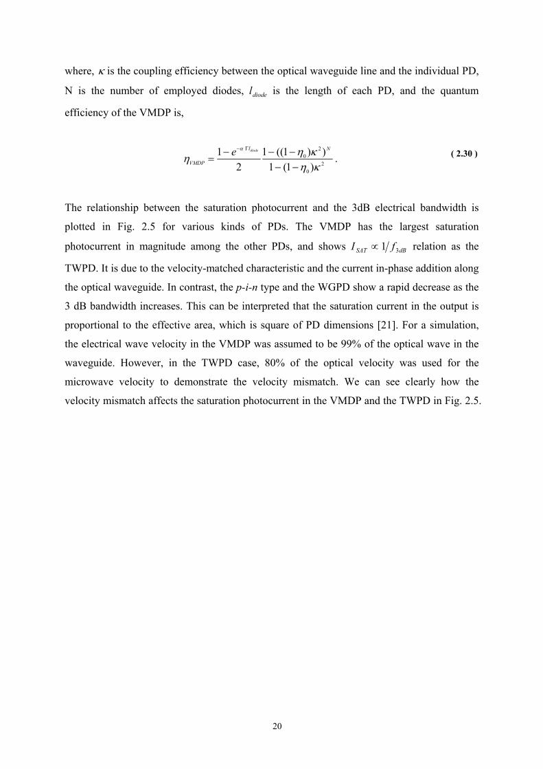
The relationship between the saturation photocurrent and the 3dB electrical bandwidth is
plotted in Fig. 2.5 for various kinds of PDs. The VMDP has the largest saturation
photocurrent in magnitude among the other PDs, and shows dBSAT fI 31∝ relation as the
TWPD. It is due to the velocity-matched characteristic and the current in-phase addition along
the optical waveguide. In contrast, the p-i-n type and the WGPD show a rapid decrease as the
3 dB bandwidth increases. This can be interpreted that the saturation current in the output is
proportional to the effective area, which is square of PD dimensions [21]. For a simulation,
the electrical wave velocity in the VMDP was assumed to be 99% of the optical wave in the
waveguide. However, in the TWPD case, 80% of the optical velocity was used for the
microwave velocity to demonstrate the velocity mismatch. We can see clearly how the
velocity mismatch affects the saturation photocurrent in the VMDP and the TWPD in Fig. 2.5.
( 2.30 )
21
Fig. 2.5 Saturation photocurrent versus bandwidth simulation. Quantum efficiency for TWPD, VMDP, and WGPD is set to 0.4. Is ( saturation phtocurrent per unit area ) is 0.025 mA/um2 [21]. The electric wave velocity Ve=0.8*Vo for TWPD, and Ve=0.99*Vo for VMDP are used, where Vo represents the optical wave velocity in the waveguide. Width = 3um, Vo=8.615E9 cm/sec [21], period=150um, length of each PD in VMDP = 15um, RL=50 Ω.
22
2.2. System model for an optically preamplified direct detection receiver system
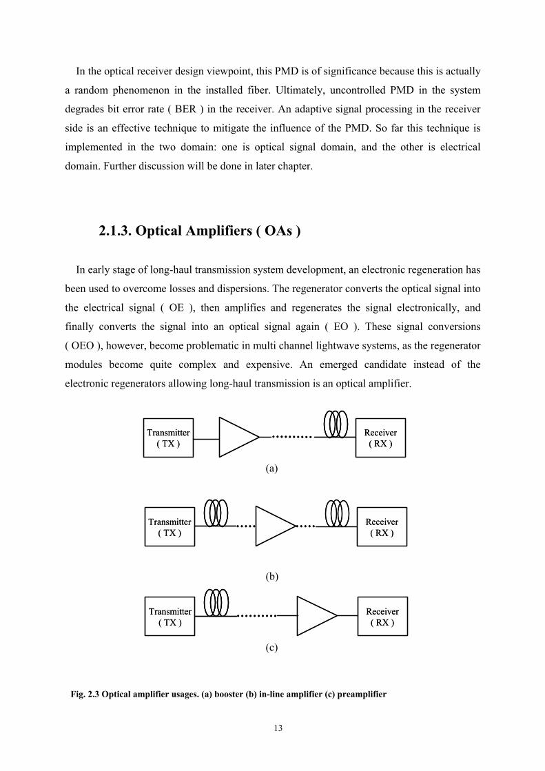
2.2.1. Introduction
The system block diagram for an optically preamplified direct detection ( OPDD ) receiver
is presented in Fig. 2.6. The light intensity is modulated in laser to transmit data stream. In
long-haul transmission system, optical amplifiers such as the Raman and(or) the EDFA
amplifier are utilized to increase optical signal power. In the OPDD system, the signal is
amplified by the EDFA ( C-band, L-band ) before the optical signal arrives the PD. In most
wavelength-division multiplexing ( WDM ) system, the optical band pass filter is located
between the EDFA and the PD. It reduces the amplified spontaneous emission ( ASE ) noise
generated in the EDFA. Regarding the ASE noise, it will be discussed in the following section.
Then, the PD directly detects the optical signal and converts into an electrical signal. The
detected electrical signal is large enough to drive the following demultiplexer circuit. Thus,
the sampling circuit based demultiplexer circuit can be directly connected to the photodetector
without further electrical amplification. In the conventional 2.5 Gbit/s and 10 Gbit/s optical
receivers without optical amplifier, the electrical current after the PD is too low for direct
digital processing in the demultiplexer and the decision circuit. Thus, so far a low noise
preamplifier and a limiting amplifier circuit have been used. Furthermore, they increase the
Fig. 2.6 System block diagram for an optically preamplified direct detection receiver with sampling circuit concept.
R
t = (k+1)Ts
fc@3dB
fc@3dBPush-push
VCO
180°
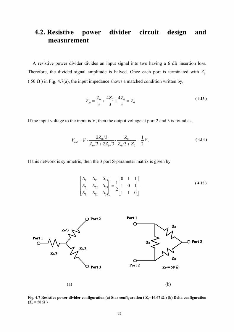
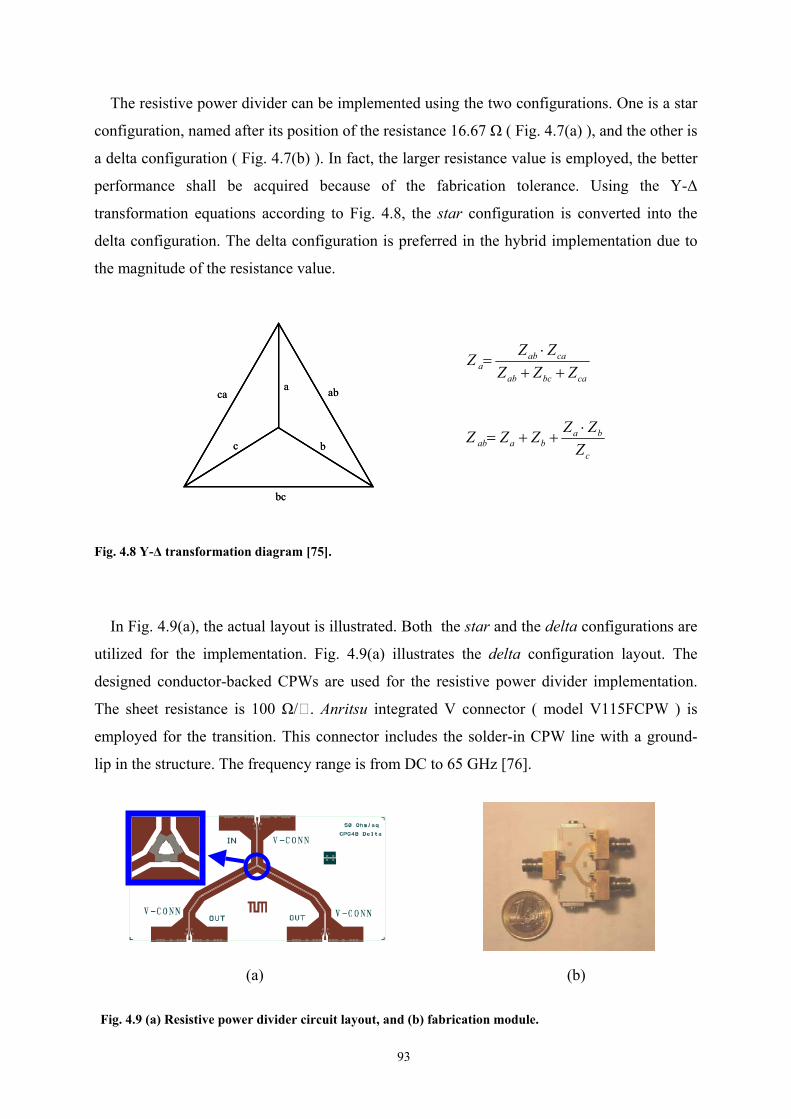
Resistive power divider
Erbium-dopedfiber amplifier
nASE
Bandpass filter
High-power photodiode
t = kTs
R
R
Equalizer
Equalizer
Phase detector Filter
R
t = (k+1)Ts
fc@3dB
fc@3dBPush-push
VCO
180°
Resistive power divider
Erbium-dopedfiber amplifier
nASE
Bandpass filter
High-power photodiode
t = kTs
R
R
Equalizer
Equalizer
Phase detector Filter
23
complexity of the optical receiver system and degrade the system performances ( power
consumption, bit error rate, etc. ). However, in the OPDD receiver system, thanks to the
optical preamplifier and the high-power PD, we expect high amplitude voltage ( current ) at
the output of the PD. The signal shall be directly processed in the following demultiplexer
circuit. We utilize this concept to construct the sampling circuit based optical receiver circuit
and illustrate this configuration in Fig. 2.6.
From the EDFA to the photodetector, it is equivalent to the conventional OPDD receiver
system. We describe here only the receiver side including the optical amplifier ( EDFA ) and
the band pass filter. It is an effective way to analyze the receiver performance excluding the
transmitter part. In this section, we describe the system model analytically for the OPDD
receiver components ( the EDFA, the optical band pass filter, and the PD ). We provide the
system characteristic functions and noise statistics when necessary. Using those analytic
descriptions above, we further present the sampling circuit based demultiplexer circuit and the
equalizer, in later sections.
2.2.1.1. System model of the EDFA
While the EDFA amplifies the optical signal, it also generates a noise component, the so-
called an amplified spontaneous emission ( ASE ) noise. It is a significant noise quantity to be
considered in a high sensitivity receiver. The EDFA can be represented equivalently with a
frequency-dependent gain ( )(υG ), and the noise figure, F . The ASE noise after signal
amplification in the EDFA is modeled as a circularly symmetric additive white Gaussian
noise process [31]. The single-sided ASE noise power spectral density is written
νννν hGnS effspASE ⋅−= )1)()(()(
where, )(νeffspn is spontaneous emission factor, )(υG is effective gain of the EDFA, h is the
Planck constant ( 6.626·10-34 J·sec ), and ν is the optical frequency. When the influence of
the incoherent background light is included in the noise power, the amplifiers’ equivalent
noise figure, equiF , is expressed as [31]
( 2.31 )
24
equibASE FGhSGS ⋅⋅⋅=⋅+ )(21)( ννν
bsp
eff
bequi ShcG
GnShFF ⋅
⋅+
−=⋅+= − λ
νννν 2
)()1)()((2)(2 1
where, F is the noise figure of the EDFA, and bS is the power spectral density ( PSD ) of the
incoherent background light.
It should be noted that relying on the signal level to be amplified in the EDFA, the
dominant noise sources are different. For a logical zero level ( ‘0’ ), a spontaneous-
spontaneous beat noise dominates, whereas a signal-spontaneous beat noise is significant for a
logical one level ( ‘1’ ). Furthermore, the probability density function ( PDF ) for each
dominating noise source has been verified theoretically as a non-Gaussian. However, the
Gaussian approximation for those noise components shows very little difference, 0.3 dB [32].
Therefore, we will use the Gaussian pdf of the ASE noise without loss of generality.
2.2.1.2. Optical band pass filters
After the broadband amplification, an optical band pass filter follows the EDFA. In the
WDM system, optical spectral filters can be classified relying on the physical phenomenon;
interference and diffraction. A typical band pass filter which takes an advantage of the
interference is the Fabry-Perot filter ( FPF ). It consists of two high-reflectance multi layers
separated by 2λ . So, spectral characteristic peaks sharply at wavelength of multiples of
2λ . Its transfer function is written below under the assumption of Lorentzian distribution,
FWHM/211
2)(
νπνααν
jjH FPF +
=+
=
where the FWHM ( πα= ) stands for full width at half maximum or at the 3dB frequency
[31][33].
The other band pass filter used in WDM system is fiber Bragg grating ( FBG ) band pass
filter. A Bragg grating is an one dimensional periodic array which has multiple semi-
( 2.32 )
( 2.33 )
( 2.34 )
25
reflectors ( reflectance R ) in its structure. Once the strong Bragg reflection condition is
satisfied shown below, a specific wavelength channel is totally reflected back to the input port.
Λ= nB 2λ
where n is the modal index, Λ is the grating period, and Bλ is the Bragg wavelength.
An example of the Bragg grating is illustrated in Fig. 2.7. The periodic structure can be
made by exposing the structure ( e.g. corrugated quaternary InxGa1-xAsyP1-y material on InP
substrate ) to the intense UV light [34]. This optical exposure technique uses a periodic
interference pattern of the light. Applying this method to the fiber, equivalently altering the
core refractive index of the fiber in a periodic way, the FBG filter can be implemented. This
filter should combine with a circulator in order to convert band stop region into band pass
filter characteristic. The optical transfer function is written as [14],
( )( ) ( )gg
gFBG
LjL
LjH
⋅−⋅−⋅−⋅−
⋅−=
222222
22
sincos
sin)(
κδδκδκδ
κδκω
where, δ is the detuning from the Bragg wavelength ( = Bλπλπ 22 − ), κ is the coupling
coefficient ( Bfibergn λπ Γ= ), and fiberΓ is the confinement factor defined as
( 2.35 )
( 2.36 )
Fig. 2.7 An example of the Bragg grating. Quaternary InxGa1-xAsyP1-y material on InP substrate is corrugated. Optical band pass filtering is illustrated for various wavelengths.
λ1 λ2 λ3 λ4
λ1 λ3 λ4
λ2
InP substrate
Λ
InxGa1-xAsyP1-y
λ1 λ2 λ3 λ4λ1 λ2 λ3 λ4
λ1 λ3 λ4λ1 λ3 λ4
λ2λ2
InP substrate
Λ
InxGa1-xAsyP1-y
InP substrate
Λ
InxGa1-xAsyP1-y
26
∫
∫∞
⋅
⋅==Γ
0
2
0
2
ρρ
ρρ
dE
dE
PP
x
a
x
total
corefiber
It is desirable to note that the bandwidth of the optical band pass filter impacts on the signal
and the noise power related with the coding scheme; non return-to-zero ( NRZ ) and return-to-
zero ( RZ ). It has been shown that ( see e.g. [35] ) for RZ signal the narrow bandwidth of the
optical filter decrease the signal energy whereas it increases the intersymbol interference
( ISI ) for NRZ. There should be a tradeoff for the NRZ coding between the ISI and the ASE-
ASE beat noise in choosing an optimum optical bandwidth of the filter. In contrast, for RZ,
the ISI does not play a significant role in determining the optimum optical bandwidth, thus the
ASE-ASE beat noise component should be considered to be minimum.
2.2.1.3. Photocurrent and noise
For the coherent electromagnetic field, the detection probability of photons is modeled by a
Poisson probability distribution. In [37], the photocurrent is considered as a stochastic process
when the photon falling at the PD is also a stochastic process. It has been shown that the
photoelectrons also have the Poisson distribution. The photoelectron generation rate is
expressed with the product of the photon arrival rate ( )(tphλ ) and the quantum efficiency of
the photon detector (η ). In this way, we can relate the photon statistics with the generated
photoelectron,
)()( tt phληλ ⋅=
where )(tphλ has the dimension of [number of photons/sec] and is defined as νhPopt . Here
optP stands for the optical power. During incremental time interval t∆ , the probability P to
find out photoelectrons is [41]
ttP ∆⋅= )(λ .
( 2.37 )
( 2.38 )
( 2.39 )
27
When photoelectrons are produced by the arrival of photons with the ratio given in ( 2.38 ),
we can assume that the electric pulse )(th with the area of q ( unit charge ) is stimulated. If
this event occurs at tkt ∆= , the pulse is delayed by tk∆ , )( tkth ∆− . Thus, electric current
)(tiPD is given by a linear superposition of the electric pulse )(th with time interval t∆ [38].
[ ]
)()(
)2()2()()()()0()()()(
tkthtkX
tthtXtthtXthXtthtXti
k
PD
∆−⋅∆=
+∆−⋅∆+∆−⋅∆+⋅+∆+⋅∆−+=
∑∞
−∞=
LL
where 1,0)( ∈⋅X is a random variable which takes ‘1’ with probability P and ‘0’ with ( 1-P ).
Ensemble average and variance of the photocurrent, which determine the statistical
characteristic of the detected photocurrent, are calculated in the following. Throughout the
derivation processes, the ⋅ symbol denotes an ensemble average.
First of all, the ensemble average of the photocurrent is expressed using the above equation
as,
( )∑∑∞
−∞=
∞
−∞=
∆−⋅∆=∆−⋅∆=kk
PD tkthtkPtkthtkXti )()()()(
Here we should note that equation ( 2.39 ) considers only one realization of the random
process. However, when we treat with the ensemble average, the probability ( )tkP ∆ is
expressed using the total probability theorem [36],
( ) ( ) ( )∫∞
∞−
== dλpkPkP λλλ
where ( )λp stands for the probability density function ( pdf ) of the random process )(tλ . By
physical interpretation, ( )λ=λkP equals to λ because the number of generated
photoelectron during time interval t∆ given the condition of photoelectron generation rate
( )tλ is ( )tλ t∆ . Therefore, the probability equals to
( 2.40 )
( 2.41 )
( 2.42 )
28
( ) λλλ =∆∆⋅
==t
tkP λ .
Inserting ( 2.43 ) into ( 2.42 ), we express the probability ( )kP as,
( ) ( ) ( ) ( ) λλλλλ =⋅=== ∫∫∞
∞−
∞
∞−
dλpdλpkPkP λ .
Inserting ( 2.44 ) into ( 2.41 ) and taking a limit as 0→∆t , we obtain the following relation,
)(*)(
)()(
)()(lim)(0
tht
dth
tkthtktiktPD
λ
τττλ
λ
=
−⋅=
∆−⋅∆=
∫
∑
∞
∞−
∞
−∞=→∆
.
The * symbol represents a convolution defined below
∫∞
∞−
−⋅= τττ dtgftgf )()())(*(
Using the following definition of the sensitivity of the photodetector,
Rq
h⋅=
νη
where R is the responsivity of the photodetector and has the unit of [ A/W ], the photoelectron
generation rate is written by,
optop
ph
PqR
hP
Rq
h
tt
⋅=
⋅
⋅=
⋅=
νν
ληλ )()(
.
( 2.43 )
( 2.44 )
( 2.45 )
( 2.46 )
( 2.47 )
( 2.48 )
29
The optical field intensity after the optical band pass filter in the optically preamplified
direct detection ( OPDD ) system is modeled as a normalized complex optical field as [47],
)()()( ttOt SIG NRX OO +=
where )(tOSIG means the complex envelope of the deterministic signal, and )(tNO stands for
the ASE noise of which characteristic is the stationary, circularly symmetric, complex
Gaussian process. It is noted that we use the bold notation in order to indicate the random
noise process. So, the optical power optP is given by
where helec BNEPRt ⋅⋅= 22 )(σ and the hB is a receiver system bandwidth. The NEP means
noise-equivalent power having a dimension of [W/Hz1/2], and it is defined below.
2
4RR
FTkNEP
L
nB
⋅⋅
=
where Bk is the Boltzmann constant ( J/K 1038066.1 23−× ), LR is the load resistance, and
nF is an equivalent amplifier noise figure. We derive the photocurrent and the noise statistics.
In the OPDD system, the noise components come from the signal amplitude dependent terms
and the stationary terms. The source signal dependent noises are composed of the signal shot
noise and the signal-ASE beat noise whereas the stationary noises are due to the ASE-ASE
beat noise and the ASE shot noise. Finally we include the electronics noise to fulfil the all
noise components. This result is summarized in ( 2.62 ).
( 2.60 )
( 2.61 )
( 2.62 )
( 2.63 )
32
2.3. Theory for the sampling circuit based demultiplexer circuit
2.3.1. Introduction
For the construction of the demultiplexing circuit, the operation principle of the sampling
circuit based demultiplexer is analyzed and the simulation is carried out. The demultiplexer
consists of a resistive power divider, two Si Schottky diode sampling circuits, and two low-
pass filters ( pulse shaping filters ) and a high-speed signal processor. In order to reduce
deterministic intersymbol interferences ( ISI ), a high-speed signal processor is connected
after each low-pass filter. In the system model, a clock oscillator signal is assumed to be
synchronous with the incoming input signal.
The amplified optical signal is incident on a waveguide-integrated high-power and high-
speed photodiode, and the measured output voltage is 200 mVpp. The electrical characteristics
of the high-speed photodiode used in the experiment are found in [25], and summarized in
Table. IV. The resistive power divider has a 6 dB insertion loss and divides the input signal
into two ways. Then, the following Si Schottky diode sampling circuit samples the dividened
signal. A sampling instant in each sampling circuit depends on the oscillator signal amplitudes.
They are out-of-phase each other, so that the sampling action takes place sequentially. The
high-speed electrical signal processor is attached to the low-pass filter following the sampling
circuit. Two algorithms for the equalizer circuit are presented; the zero-forcing algorithm and
the Wiener-Kolmogorov algorithm.
Table. IV Electrical characteristics of the high-speed photodiode used in the experiment [25]
Terms Value
3 dB bandwidth > 50 GHz
Pulse width ( typ. ) 9 ps
Wavelength range 1480~1620 nm
Polarization dependent loss ( dB ) 0.5 ( typ )
Dark current 5 nA
Max. optical input power 13 dBm
S22 ( 0.05~50 GHz ) -13 dB
33
2.3.2. Theory description
For the purpose of the description about the sampling circuit based demultiplexer circuit,
we will use a time-limited signal, )(tORX and generalize the analytic pulse expression for
both the NRZ and the RZ signal. We temporarily consider only optical signal field excluding
the random noise component for circuit’s functional explanation. Thus, we would use scalar
notation for the signal after the optical band pass filter, i.e. )(tO(t)O SIGRX = . Let the optical
field be defined within the time interval [0, (1+α)Tp],
+≤≤⋅≤≤
−+−
⋅−⋅
⋅
≤≤⋅
=
otherwise0
)1(or0for22
)1(sin12
for
)( 1
1
ppppp
pp
ppp
RX TtTTtTT
tTT
E
TtTTE
tO ααααπ
α
where, E1 denotes the optical energy for a ‘1’ bit, and Tp is the effective pulse duration shown
below [31].
( ) ( ))(max)(max
)(1
tOE
tO
dttOT
RXtRXt
RX
p ==∫∞
∞−
Varying the pulse width with α and Tp, the NRZ and RZ pulse shape can be acquired. For
example,
⋅=
signalRZforTdsignalNRZforT
Tbit
bitp
where, bitT is a bit duration, and d is the duty cycle, 33% [31]. Using the above equation, the
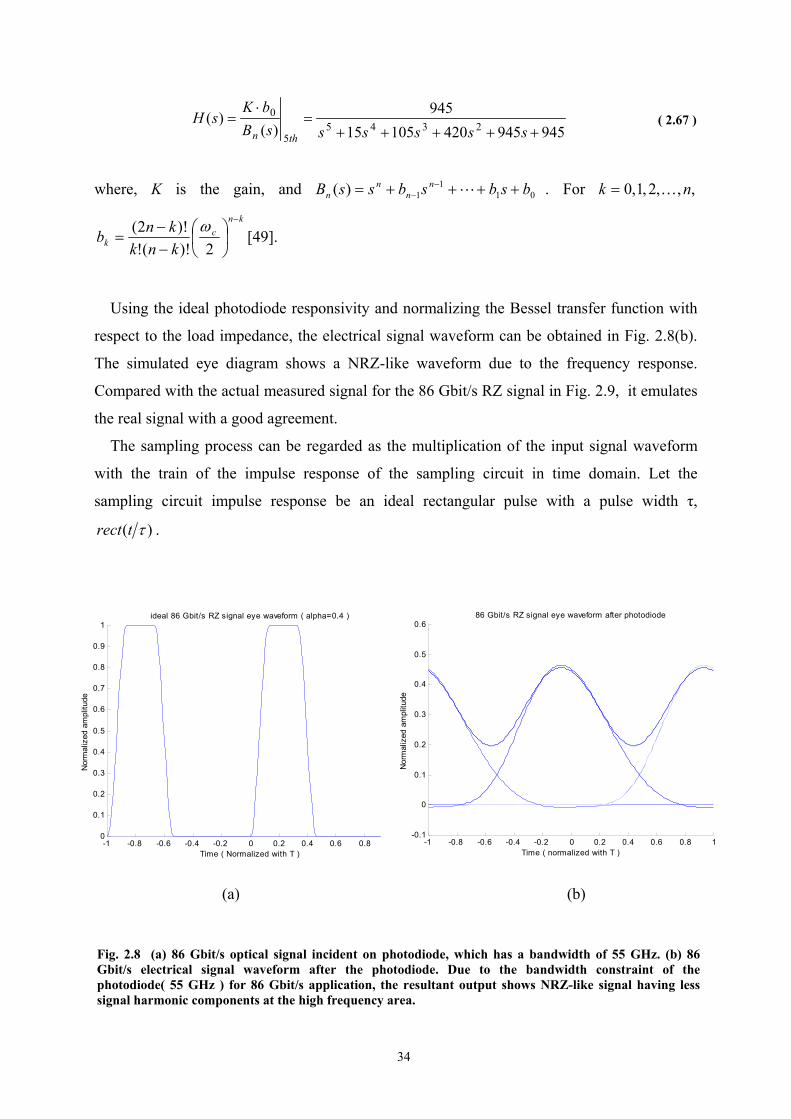
optical pulse of 86 Gbit/s RZ optical signal is depicted in Fig. 2.8(a). Representing the
frequency response of the photodiode and the electrical connector as a 5th order Bessel filter,
its transfer function can be written as,
( 2.64 )
( 2.65 )
( 2.66 )
34
94594542010515945
)()(
23455
0
+++++=
⋅=
ssssssBbK
sHthn
where, K is the gain, and 011
1)( bsbsbssB nn
nn ++++= −
− L . For ,,,2,1,0 nk K=
knc
k knkknb
−
−−
=2)!(!
)!2( ω[49].
Using the ideal photodiode responsivity and normalizing the Bessel transfer function with
respect to the load impedance, the electrical signal waveform can be obtained in Fig. 2.8(b).
The simulated eye diagram shows a NRZ-like waveform due to the frequency response.
Compared with the actual measured signal for the 86 Gbit/s RZ signal in Fig. 2.9, it emulates
the real signal with a good agreement.
The sampling process can be regarded as the multiplication of the input signal waveform
with the train of the impulse response of the sampling circuit in time domain. Let the
sampling circuit impulse response be an ideal rectangular pulse with a pulse width τ,
)( τtrect .
(a) (b)
( 2.67 )
Fig. 2.8 (a) 86 Gbit/s optical signal incident on photodiode, which has a bandwidth of 55 GHz. (b) 86 Gbit/s electrical signal waveform after the photodiode. Due to the bandwidth constraint of the photodiode( 55 GHz ) for 86 Gbit/s application, the resultant output shows NRZ-like signal having less signal harmonic components at the high frequency area.
-1 -0.8 -0.6 -0.4 -0.2 0 0.2 0.4 0.6 0.8 10
0.1
0.2
0.3
0.4
0.5
0.6
0.7
0.8
0.9
1
Time ( Normalized with T )
Nor
mal
ized
am
plitu
de
ideal 86 Gbit/s RZ signal eye waveform ( alpha=0.4 )
-1 -0.8 -0.6 -0.4 -0.2 0 0.2 0.4 0.6 0.8 1-0.1
0
0.1
0.2
0.3
0.4
0.5
0.686 Gbit/s RZ signal eye waveform after photodiode
Time ( normalized with T )
Nor
mal
ized
am
plitu
de
35
The input signal to the demultiplexer can be expressed as
∑∞
=
−⋅=⋅0
)()(),(n
bitn nTtgrtd
where, )(⋅nr represents all possible ensembles of a random variable 1,exγ with a extinction
ratio exγ . The extinction ratio is defined as
101
0 ≤=≤PP
exγ
where 0P is the power emitted during logical level ‘0’, and 1P is for the level ‘1’. Here, we
use the normalized 1P value. And, )(tg can be expressed as a convolution of )(tORX and
)(th of the inverse Laplace transform of the 5th order Bessel filter.
Thus,
∫∞
−∞=−⋅⋅⋅=⋅⋅=
ττττ dthORZthtORZtg RXLRXL )()()(*)()( 22
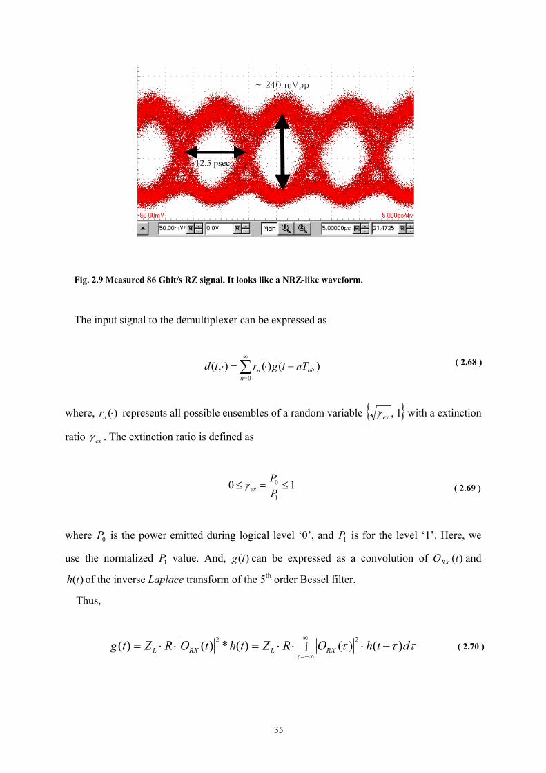
Fig. 2.9 Measured 86 Gbit/s RZ signal. It looks like a NRZ-like waveform.
( 2.68 )
( 2.69 )
( 2.70 )
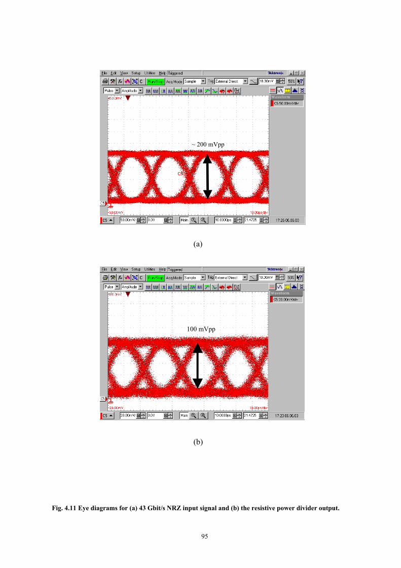
~ 240 mVpp
~12.5 psec
36
where )()( 1 sHLth −= , R , and LZ are the responsivity and a load impedance of the PD.
Using a pulse shaping function, )(tg , a code length of 128 − PRBS data waveform is
generated shown in Fig. 2.10(a) and depicts a logical value, ‘1’, or ‘0’ on each signal.
The sampling circuit output signals, channel 1 and channel 2, can be expresses as,
+−
⋅−⋅⋅⋅=⋅⋅+−⋅=
−
⋅−⋅⋅⋅=⋅⋅−⋅=
∑
∑
∞
=
∞
=
TTntrectnTtgrtdTnthtS
TnTtrectnTtgrtdnTthtS
nntrainChsampler
nntrainChsampler
)12()()(21),())12((2
1)(
2)()(21),()2(2
1)(
02.
01.
where, ∑ ∑∞
=
∞
=
−
=−=0 0
)()(n n
train TnTtrectnTthth is the impulse train of the sampling
circuit, illustrated in Fig. 2.10(b). Fig. 2.10(c) depicts its sampled signal waveform, and they
are ideally similar to the rectangular pulses. Comparing with the input signal waveform in Fig.
2.10(a), the output waveform clearly explains that every second bits in the input data stream
are detected. The sampled signal should be processed with the low-pass filter to make a
demultiplexed waveform. It is simulated using the 5th order Bessel filter, which has a
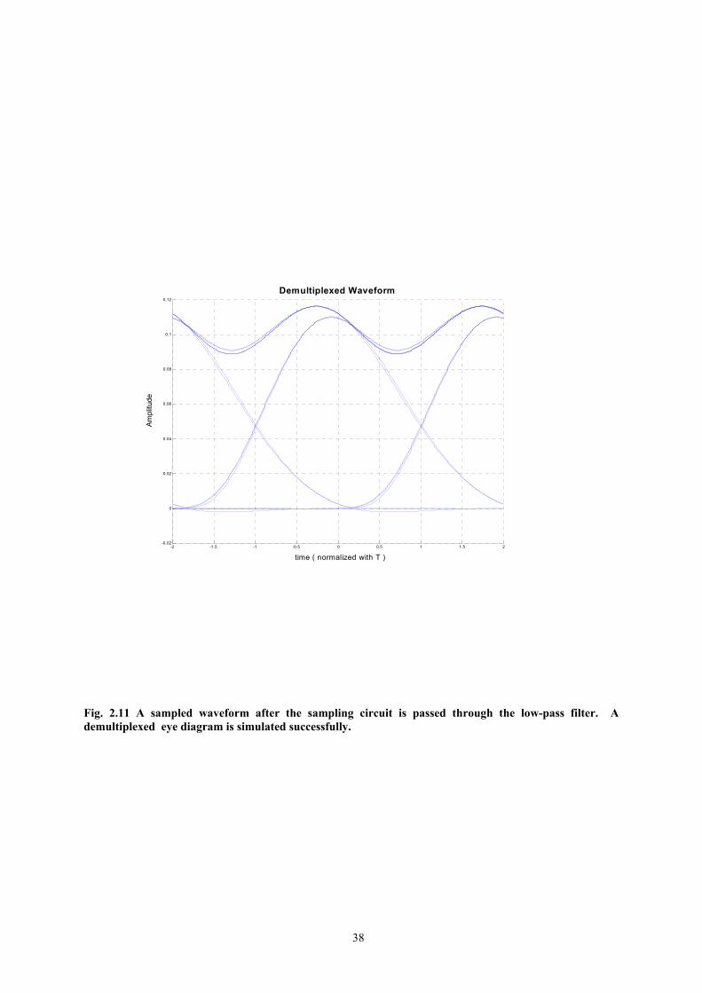
bandwidth of 20 GHz. Therefore, the demultiplexed output signal is written as a convolution
where )(thLPF is the low-pass filter transfer function with 20 GHz bandwidth. Simulation
result is presented in Fig. 2.11. It illustrates a demultiplexed pulse width ( ~20psec, 40
Gbit/s ) and NRZ-like waveform. A MATLAB program is presented in Appendix B.
So far, we explain the sampling circuit based receiver circuit theory in detail using the ideal
sampling circuit impulse response ( rectangular function in time domain ). We successfully
acquire the demultiplexed digital eye waveform. It should be noted that the sampling in the
sampling circuit does mean literally detecting the electrical signal periodically for
demultiplexing purpose. It differs from the sampling in Nyquist theorem which defines the
minimum sampling frequency to reconstruct the original signal without aliasing effect.
( 2.71 )
( 2.72 )
37
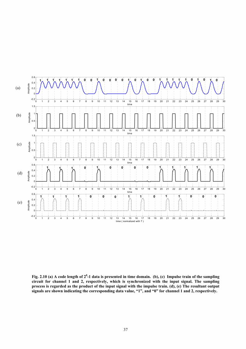
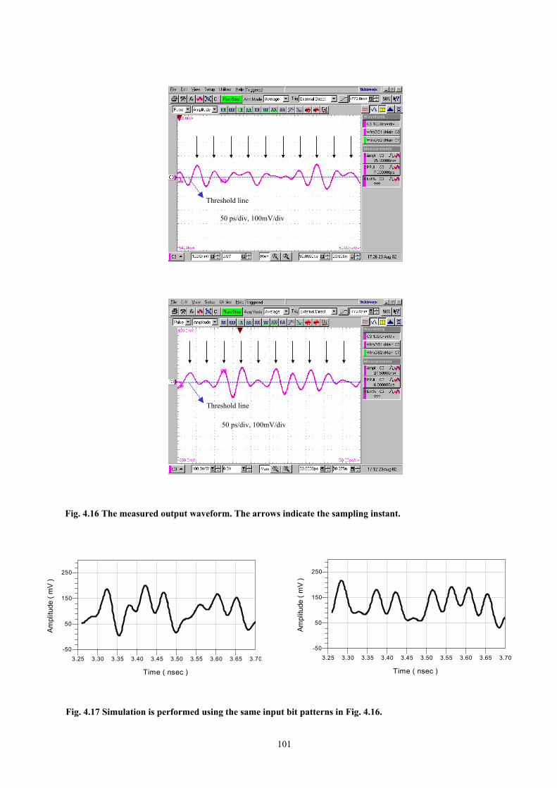
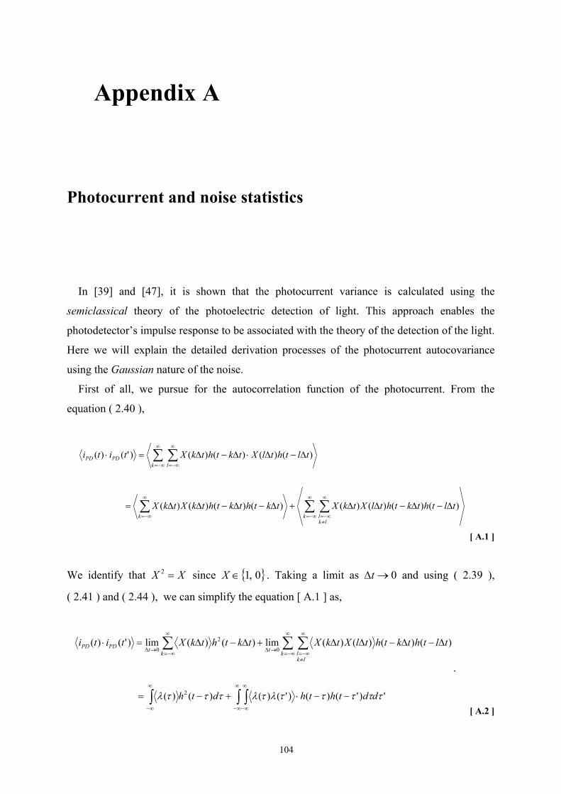
Fig. 2.10 (a) A code length of 28-1 data is presented in time domain. (b), (c) Impulse train of the sampling circuit for channel 1 and 2, respectively, which is synchronized with the input signal. The sampling process is regarded as the product of the input signal with the impulse train. (d), (e) The resultant output signals are shown indicating the corresponding data value, “1”, and “0” for channel 1 and 2, respectively.
And, we can also write the above equation using the transfer function ( )(th ) in matrix form,
ηsH
nHsHsDEM
+⋅=
⋅+⋅=
where, 1×∈ MCsDEM , T21 ][ Nk ssss LL=s , 1×∈ NCn , NM ×∈CH , and we assume 0n =E
After the equalizer, the output signal is given as
ηGsHG
ηsHGs
HH
Hout
⋅+⋅⋅=
+⋅⋅= )(
,
where G is the transfer function of the equalizer circuit, and NM×∈CG . The symbol H)(⋅
means the Hermitian matrix, a combined operation of transpose and complex conjugation.
The kth element of outs is given by
32144 344 21
43421noise
ISIsignaldesired
ˆ1
, ηGhGhG Hki
Hkk
Hk ⋅+⋅⋅+⋅⋅= ∑
≠=
N
kii
ikkout sss
where Nk21 GGGGG KK ,,,,= , [ ]T,,1, ,,, kLkLkL ggg K+−−=kG , Nk21 hhhhH ,,,,, KK= ,
[ ]T,1,1,0 ,,, kMkk hhh −= Kkh , and 12 += LM .
The zero-forcing filter is defined as an equalizer to eliminate the ISI component. It is also
called as the peak distortion criterion, because it minimize the peak distortion defined by the
ISI. Assuming the infinite number of filter coefficients, the kth output signal is acquired as
( 2.76 )
( 2.77 )
( 2.78 )
( 2.79 )
43
ηG Hk ⋅+= kkout ss ,ˆ
Therefore, if the following condition is satisfied
NH IHG =⋅
where,
=
1
11
N
0
0
IO
,
we can obtain the ISI-free signal after the equalizer. Fig. 2.13 illustrates a filter based on the
zero-forcing algorithm with order of ( 2N+1 ). It consists of periodic delay lines and
coefficient multipliers. At this moment filter coefficients are fixed to a certain value, however
if we apply the adaptive signal processing technique to the filter, coefficients are adaptively
changed.
The zero-forcing filter coefficients are decided by the following argument.
NHH subject to )( min arg IHGGRG ηG
=⋅⋅⋅tr
where, HHHE HRHHnnHR nη ⋅⋅=⋅⋅= , and H E nnRn = is a noise correlation vector.
The )(⋅tr symbol represents a trace of a matrix.
Fig. 2.13 Linear equalizer. Coefficients are calculated using the Zero-forcing algorithm.
( 2.80 )
( 2.81 )
( 2.82 )
Z-1
Σ
Z-1Input Z-1 Z-1
gLgL-1g-L+1g-L g-L+2
Output
Z-1
Σ
Z-1Input Z-1 Z-1
gLgL-1g-L+1g-L g-L+2
Output
44
Minimizing the noise power, )( H GRG η ⋅⋅tr at the output of the equalizer circuit, we
calculate filter coefficients. This is a constrained minimization problem, which can be solved
using the Lagrange multipliers method. The Lagrangian equation is
λIHGIGHλGRGλG η ⋅−⋅+−⋅⋅+⋅⋅= )()()(),(N
HN
HHHtrL ,
where λ is a Lagrange multiplier in vector form.
Finding out the conditions for 0),(
* =G
λG
d
dL and 0
),(* =
λ
λG
d
dL, the following result can be
derived,
11H1
ZF)( −−− ⋅⋅= HRHHRG ηη .
If N
2 IR η nσ= , the zero-forcing filter coefficient vector is found as += )( H
ZFHG . Here, the
(·)+ symbol represents the pseudo-inverse matrix.
Using the above result, we can calculate the SNR at the output of the filter. We will derive
the expressions for the signal power and the noise power, respectively. First of all, the signal
power after the equalization
Ntr === H22EQs, EEP sss .
Here we normalize the signal power and assume the infinite number of filter coefficients.
And, the noise power is given
( ) ( )
( ) 1H
1HH1HHEQN,P
−
−−
⋅=
⋅⋅⋅⋅=
⋅⋅=
HH
HHHHHHGRG η
tr
trtr
Let us decompose ( ) 1H −⋅HH using the singular value decomposition ( SVD ). It is shown that
if HUΛUHH ⋅⋅=⋅H where Λ is given by,
( 2.83 )
( 2.84 )
( 2.85 )
( 2.86 )
45
=
Nλ
λλ
0
0
ΛO
2
1
with eigenvalues of the matrix ),,,( 21 Nλλλ K , then
( ) HUΛUHH ⋅⋅=⋅ −− 11H .
Thus, the noise power is calculated as
∑=
=N
k k1EQN,
1Pλ
.
We therefore obtain the SNR as
∑=
== N
k k
EQN
EQs NPP
1
,
,
1SNR
λ
.
If CN λλλλ ==== L21 , then the SNR simply equals to cλ .
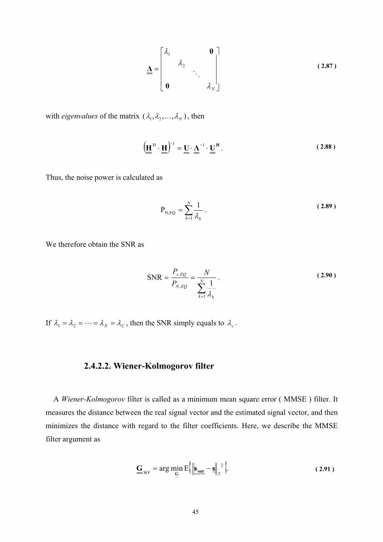
2.4.2.2. Wiener-Kolmogorov filter
A Wiener-Kolmogorov filter is called as a minimum mean square error ( MMSE ) filter. It
measures the distance between the real signal vector and the estimated signal vector, and then
minimizes the distance with regard to the filter coefficients. Here, we describe the MMSE
filter argument as
2
2WFEmin arg ssG outG
−= .
( 2.87 )
( 2.88 )
( 2.89 )
( 2.90 )
( 2.91 )
46
The solution for the above argument can be obtained when the first differentiation
0Gssout =− *2
2E dd .
A function for the vector norm is given by
( ) ( )
HHHH
H
E EEE
E)K(
ssssssss
ssssG
outoutoutout
outout
⋅−⋅−⋅−⋅=
−⋅−=
trtrtrtr
tr
If we assume that the signal and the noise is uncorrelated each other, and using facts below,
Ntrtr ==
⋅+⋅⋅=
NH
HH
E Iss
ηGsHGsout
we express the vector norm function as
( ) ( ) Ntrtrtr +⋅−⋅−
+= GHHGGRHHGG η
HHHH)K(
Solving 0GG =*)(K dd , the MMSE filter condition is calculated as shown below,
( )
+⋅=
−
ηRHHHG1H
WF.
To compare this solution with the zero-forcing algorithm solution, let us use the matrix
identity below.
( ) ( ) 111H11H −−−−−+≡+ BACAACBACABA
Setting HA = , N
IB = , and ηRC = , and inserting to the above equation, the final result is
( 2.92 )
( 2.93 )
( 2.94 )
( 2.95 )
( 2.96 )
( 2.97 )
47
straightforward.
1
N1H1
WF
−−−
+= IHRHHRG ηη
In general, when the transmit power increases, the MMSE filter solution approaches to the
zero-forcing solution while the decreased signal power causes the MMSE filter coefficients
converging to the matched filter coefficients.
For the sampling circuit based demultiplexer circuit, two algorithm for the equalizer circuit
are presented. Using a finite number of taps the equalizer circuit for the demultiplexer circuit
will be proposed and simulated. That is discussed in section 3.4.2.
( 2.98 )
48
3.1. Si Schottky diode modeling
Schottky diodes are majority carrier devices, and as a consequence a storage time due to
minority carriers is quite small, i.e., resulting in little diffusion capacitance. A junction
capacitance dominates in forward bias condition. Hence, the diode shows ultra-fast switching
speed compared to other junction diodes. This is an attractive advantage for millimeter-wave
circuit design. Very high-speed Schottky diodes having cutoff frequencies in THz regime are
reported in [9] and [10] using Si and III-V compound semiconductor materials.
Concerning the Schottky diode model, a large-signal nonquasi-static model should be
considered in high frequency regime. Nonquasi-static device modeling is desirable when the
operating frequency approaches the upper limit of validity for quasi-static models.
Chapter 3 Circuit Design and
Simulation
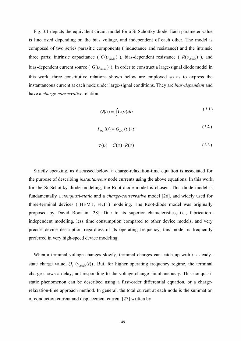
Fig. 3.1 Equivalent circuit of a diode. It is composed of extrinsic components ( L, R ) and the intrinsic components )( diodeC υ , )( diodeR υ , and )( diodeG υ , which are bias-dependent and specified independently.
L R
)( diodeC υ )( diodeR υ
)( diodeG υ
+ −diodeυ
Anode Cathode
49
Fig. 3.1 depicts the equivalent circuit model for a Si Schottky diode. Each parameter value
is linearized depending on the bias voltage, and independent of each other. The model is
composed of two series parasitic components ( inductance and resistance) and the intrinsic
three parts; intrinsic capacitance ( )( diodeC υ ), bias-dependent resistance ( )( diodeR υ ), and
bias-dependent current source ( )( diodeG υ ). In order to construct a large-signal diode model in
this work, three constitutive relations shown below are employed so as to express the
instantaneous current at each node under large-signal conditions. They are bias-dependent and
have a charge-conservative relation.
∫= υυυ dCQ )()(
υυυ ⋅= )()( DCDC GI
)()()( υυυτ RC ⋅=
Strictly speaking, as discussed below, a charge-relaxation-time equation is associated for
the purpose of describing instantaneous node currents using the above equations. In this work,
for the Si Schottky diode modeling, the Root-diode model is chosen. This diode model is
fundamentally a nonquasi-static and a charge-conservative model [26], and widely used for
three-terminal devices ( HEMT, FET ) modeling. The Root-diode model was originally
proposed by David Root in [28]. Due to its superior characteristics, i.e., fabrication-
independent modeling, less time consumption compared to other device models, and very
precise device description regardless of its operating frequency, this model is frequently
preferred in very high-speed device modeling.
When a terminal voltage changes slowly, terminal charges can catch up with its steady-
state charge value, ))(( tvQ diodesss . But, for higher operating frequency regime, the terminal
charge shows a delay, not responding to the voltage change simultaneously. This nonquasi-
static phenomenon can be described using a first-order differential equation, or a charge-
relaxation-time approach method. In general, the total current at each node is the summation
of conduction current and displacement current [27] written by
( 3.1 )
( 3.2 )
( 3.3 )
50
)()()( tItItI dispcondtotal +=
where ))(()( tvItI diodeocond = , dttdQtI disp )()( = , and )(tQ is the node charge.
Using a charge-relaxation-time approach, )(tI disp can be expressed using the following
equation.
)))((),((())(()()()(tvRtvC
tvQtQdt
tdQtIdiodediode
diodesss
disp τ−
−==
Note that the applied bias to the diode neglects voltage drops at the parasitic resistance for
simplicity. Equation ( 3.5 ) describes the large-signal behavior of the displacement current,
and also enables to determine the nonquasi-static characteristic of the diode. This Root-diode
model can be used for transient analysis in time domain, harmonic balance simulation in
frequency domain, and small-signal analysis in frequency domain [28].
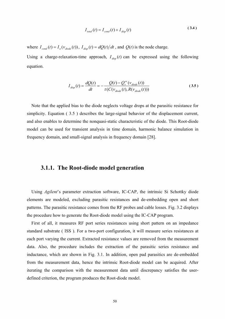
3.1.1. The Root-diode model generation
Using Agilent’s parameter extraction software, IC-CAP, the intrinsic Si Schottky diode
elements are modeled, excluding parasitic resistances and de-embedding open and short
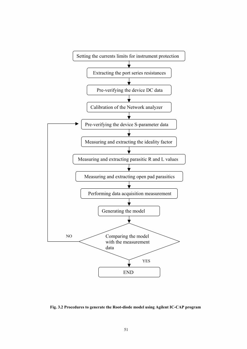
patterns. The parasitic resistance comes from the RF probes and cable losses. Fig. 3.2 displays
the procedure how to generate the Root-diode model using the IC-CAP program.
First of all, it measures RF port series resistances using short pattern on an impedance
standard substrate ( ISS ). For a two-port configuration, it will measure series resistances at
each port varying the current. Extracted resistance values are removed from the measurement
data. Also, the procedure includes the extraction of the parasitic series resistance and
inductance, which are shown in Fig. 3.1. In addition, open pad parasitics are de-embedded
from the measurement data, hence the intrinsic Root-diode model can be acquired. After
iterating the comparison with the measurement data until discrepancy satisfies the user-
defined criterion, the program produces the Root-diode model.
( 3.4 )
( 3.5 )
51
Setting the currents limits for instrument protection
Extracting the port series resistances
Pre-verifying the device DC data
Calibration of the Network analyzer
Pre-verifying the device S-parameter data
Measuring and extracting the ideality factor
Measuring and extracting parasitic R and L values
Measuring and extracting open pad parasitics
Performing data acquisition measurement
Generating the model
Comparing the model with the measurement data
END
NO
YES
Fig. 3.2 Procedures to generate the Root-diode model using Agilent IC-CAP program
52
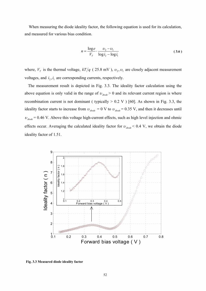
When measuring the diode ideality factor, the following equation is used for its calculation,
and measured for various bias condition.
12
12
logloglog
iiVen
T −−
⋅=υυ
where, TV is the thermal voltage, qkT ( 25.8 mV ), 12 ,υυ are closely adjacent measurement
voltages, and 12 , ii are corresponding currents, respectively.
The measurement result is depicted in Fig. 3.3. The ideality factor calculation using the
above equation is only valid in the range of diodeυ > 0 and its relevant current region is where
recombination current is not dominant ( typically > 0.2 V ) [60]. As shown in Fig. 3.3, the
ideality factor starts to increase from diodeυ = 0 V to diodeυ = 0.35 V, and then it decreases until
diodeυ = 0.46 V. Above this voltage high-current effects, such as high level injection and ohmic
effects occur. Averaging the calculated ideality factor for diodeυ < 0.4 V, we obtain the diode
ideality factor of 1.51.
( 3.6 )
Fig. 3.3 Measured diode ideality factor
0.1 0.2 0.3 0.4 0.5 0.6 0.7 0.81
2
3
4
5
6
7
8
9
Forward bias voltage ( V )
Idea
lity
fact
or (
n )
0.1 0.2 0.3 0.4 0.51
1.2
1.4
1.6
1.8
2
Forward bias voltage ( V )
Idea
lity
fact
or (
n )
53
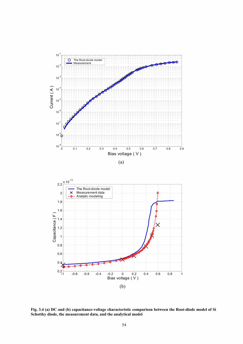
Fig. 3.4(a) shows the I-V curve comparing measurement results with the modeling data.
They show excellent agreement in the whole measurement range. And, the C-V characteristic
curve is shown in Fig. 3.4(b). We compare the Root-diode model, the measurement data, and
an analytic modeling equation. In order to determine parameters in the analytical expression,
we fit the equation ( 3.7 ) to the measurement data,
γ
Φ−=
bi
V
CVC1
)0()(
where the zero voltage capacitance )0(C is 47 fF, the built-in potential biΦ is 0.63 V, and the
junction grading coefficient γ is 0.5 [61].
The comparison between the Root-diode model, the measurement data, and the analytical
modeling data looks quite good below the forward bias of 0.2 V. In general as the forward
bias increases, the diffusion capacitance increases while the junction capacitance dominates in
the reverse bias condition. The slight deviation from the Root-diode model is attributed to the
parasitic voltage drop due to the parasitic resistance in probes and the extrinsic device series
resistance. Thus, the diffusion capacitance is lower than the Root-diode model data.
Effective barrier height calculation is straightforward using a Schottky barrier diode I-V
relation,
−
⋅
∆Φ−−⋅⋅= 1expexp2**
nkTqV
nkTTAJ B
sφ
where Bφ is the barrier height of a Schottky junction, ∆Φ is an effective barrier lowering due
to the image force effect, and **A is an effective Richardson constant, which is assumed to be
unaffected by the tunneling process ( 112 22/ TcmA ⋅ ). We obtain the effective barrier height
( ∆Φ−Bφ ) of 0.53 eV using the measured DC I-V relation.
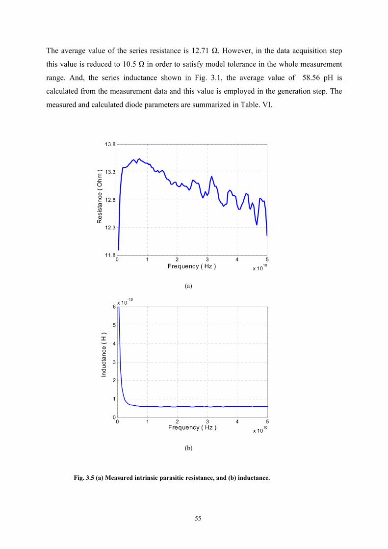
The parasitic intrinsic series resistance and inductances are also measured varying the
frequency up to 50 GHz. When performing data acquisition measurement in the Root-diode
model generation, as described in Fig. 3.5, the average values are used to accommodate error
tolerances in the actual model.
( 3.7 )
( 3.8 )
54
(a)
(b)
Fig. 3.4 (a) DC and (b) capacitance-voltage characteristic comparison between the Root-diode model of Si Schottky diode, the measurement data, and the analytical model
0 0.1 0.2 0.3 0.4 0.5 0.6 0.7 0.8 0.910
-9
10-8
10-7
10-6
10-5
10-4
10-3
10-2
10-1
Bias voltage ( V )
Cur
rent
( A
)
The Root-diode model Measurement
-1 -0.8 -0.6 -0.4 -0.2 0 0.2 0.4 0.6 0.8 10.2
0.4
0.6
0.8
1
1.2
1.4
1.6
1.8
2
2.2x 10
-13
Bias voltage ( V )
Cap
acita
nce
( F )
The Root-diode modelMeasurement data Analytic modeling
55
The average value of the series resistance is 12.71 Ω. However, in the data acquisition step
this value is reduced to 10.5 Ω in order to satisfy model tolerance in the whole measurement
range. And, the series inductance shown in Fig. 3.1, the average value of 58.56 pH is
calculated from the measurement data and this value is employed in the generation step. The
measured and calculated diode parameters are summarized in Table. VI.
(a)
(b)
Fig. 3.5 (a) Measured intrinsic parasitic resistance, and (b) inductance.
0 1 2 3 4 5
x 1010
11.8
12.3
12.8
13.3
13.8
Frequency ( Hz )
Res
ista
nce
( Ohm
)
0 1 2 3 4 5
x 1010
0
1
2
3
4
5
6x 10
-10
Frequency ( Hz )
Indu
ctan
ce (
H )
56
Terms Value
Ideality factor 1.51
Effective barrier height 0.63 eV Contact metal Ni silicide
Capacitance at zero bias 48 fF
Grading coefficient 0.5
Reverse saturation current, Is 2.7 nA
Series resistance 10.5 Ω
Series inductance 58.6 pH
Cutoff frequency 320 GHz
Table. VI. Measured diode model parameters ( diode area : 4.5 µm x 4.5 µm )
57
3.2. Flip-chip equivalent circuit modeling
In the thin-film fabrication technology, a flip-chip bonding is an important method to
mount passive and active components on the same substrate. This mounting technique also
allows to increase system performance, and simultaneously reduce cost compared to
monolithic implementations. However, for the microwave and millimeter wave applications,
the flip-chip bonding interconnect causes parasitic components due to its inherent bonding
nature, namely, dielectric chip overloading on motherboard substrate, and bonding bump
transition from the chip to the substrate [44]. Even though flip-chip bonding parasitics are not
sufficiently large enough to deteriorate signal integrity in the low frequency or at some
specific frequency area, they are to be extensively studied in case of broad and baseband
signal case. They have frequency dependent behavior, therefore causing signal distortion
depending on frequency, and also producing resonance phenomenon in the frequency region
of interest.
In order to set up the flip-chip bonding model, a 3-dimensional electromagnetic simulator,
Ansoft HFSS, is utilized for equivalent circuit modeling. In [43], an equivalent circuit model
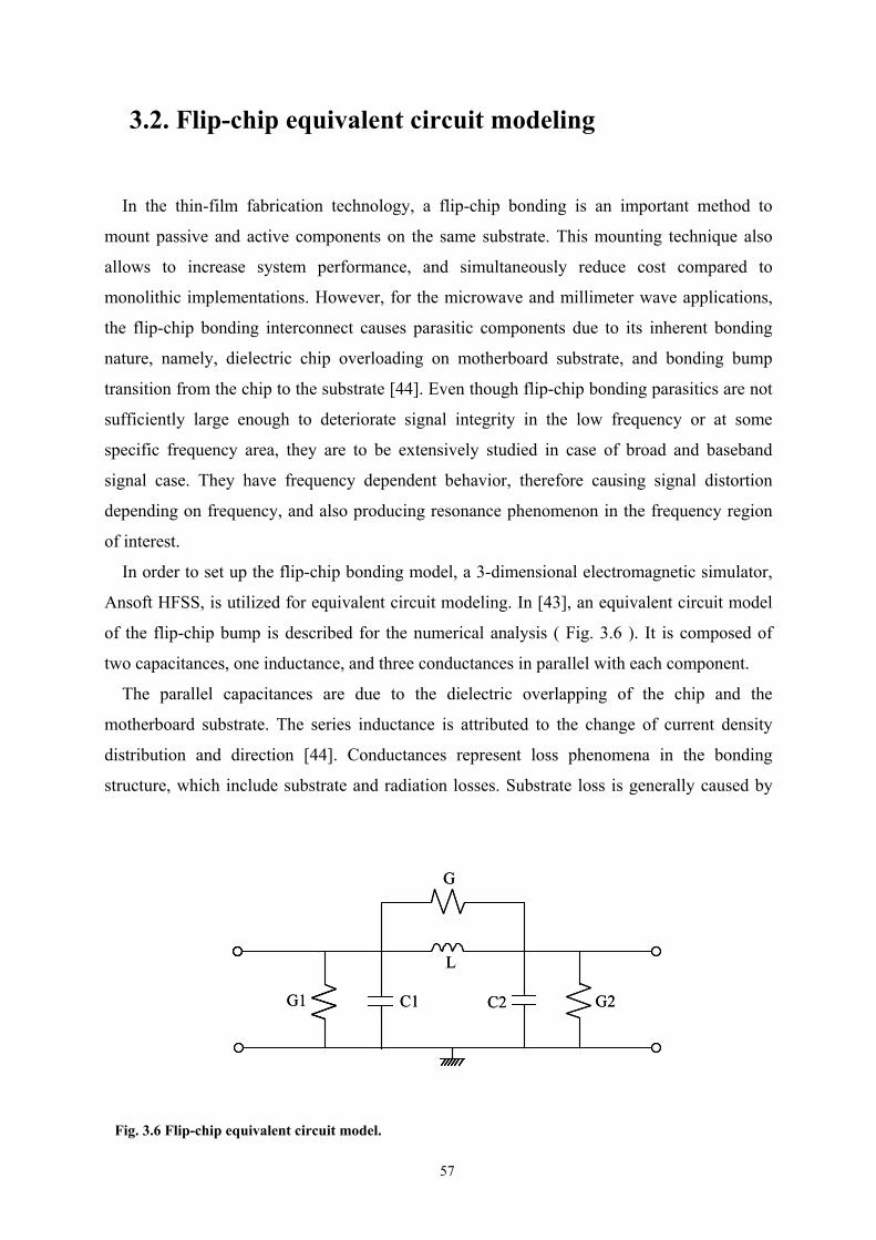
of the flip-chip bump is described for the numerical analysis ( Fig. 3.6 ). It is composed of
two capacitances, one inductance, and three conductances in parallel with each component.
The parallel capacitances are due to the dielectric overlapping of the chip and the
motherboard substrate. The series inductance is attributed to the change of current density
distribution and direction [44]. Conductances represent loss phenomena in the bonding
structure, which include substrate and radiation losses. Substrate loss is generally caused by
Fig. 3.6 Flip-chip equivalent circuit model.
G
G2G1 C1 C2
L
G
G2G1 C1 C2
L
58
the excitation of surface waves in the substrate. Radiation loss stems from the energy loss of
radiated electromagnetic waves from the bump [43]. In this work, those losses are neglected,
hence only two capacitances and one inductance are considered in the equivalent circuit
modeling of the flip-chip bonding connection.
Since there are one inductance and two capacitances in the circuit model, two resonance
frequencies are analytically found. If one port is terminated with 0Z , the first resonance
frequency is Hz0=resf and the second is
+−
++
−=
)(41
2221
12
221
21
12
21
12
CCLZCC
ZCCCC
ZCCCCf o
oores π
.
In the transverse direction of the bump transition, 0Z approaches ∞ [30]. In this case a
transverse resonance frequency is located at
( )2121
21, ||
121
21
CCLLCCCCf transverseres ππ
=+
= .
Various methods to reduce return loss due to the flip-chip bump transition have been
developed. For example, a staggered bump method and an insertion of a hi-impedance line in
order to compensate capacitive behavior of the flip-chip [46]. Those geometrical approaches
are fundamentally intended to change the resonance frequency or to add ( or reduce ) the
discrete component. It is reported that the return loss can remain below –20 dB until 82 GHz
using the compensation method [46].
3.2.1. Simulation of the flip-chip bonding connection
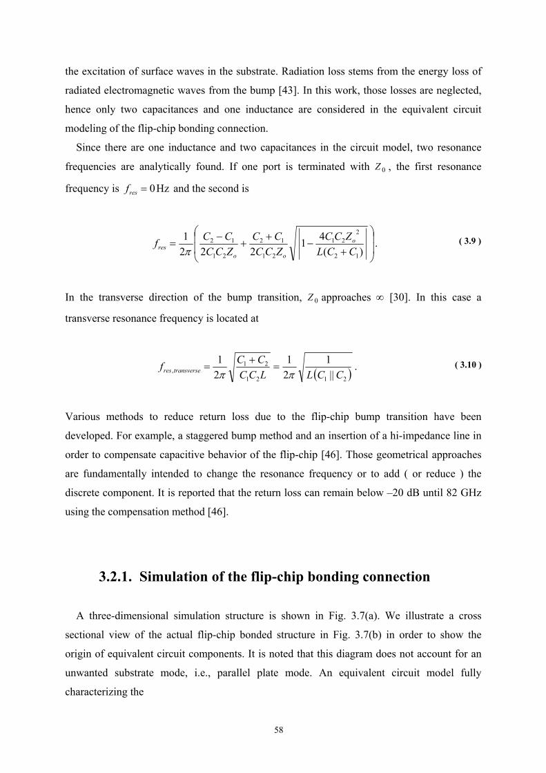
A three-dimensional simulation structure is shown in Fig. 3.7(a). We illustrate a cross
sectional view of the actual flip-chip bonded structure in Fig. 3.7(b) in order to show the
origin of equivalent circuit components. It is noted that this diagram does not account for an
unwanted substrate mode, i.e., parallel plate mode. An equivalent circuit model fully
characterizing the
( 3.9 )
( 3.10 )
59
(a)
(b)
flip-chip bonding including higher order modes is under research. However, the flip-chip
employed circuit generally operates within a certain frequency range where higher order
electromagnetic modes start to occur. Thus, it is still useful to use discrete equivalent circuit
model for circuit design purposes.
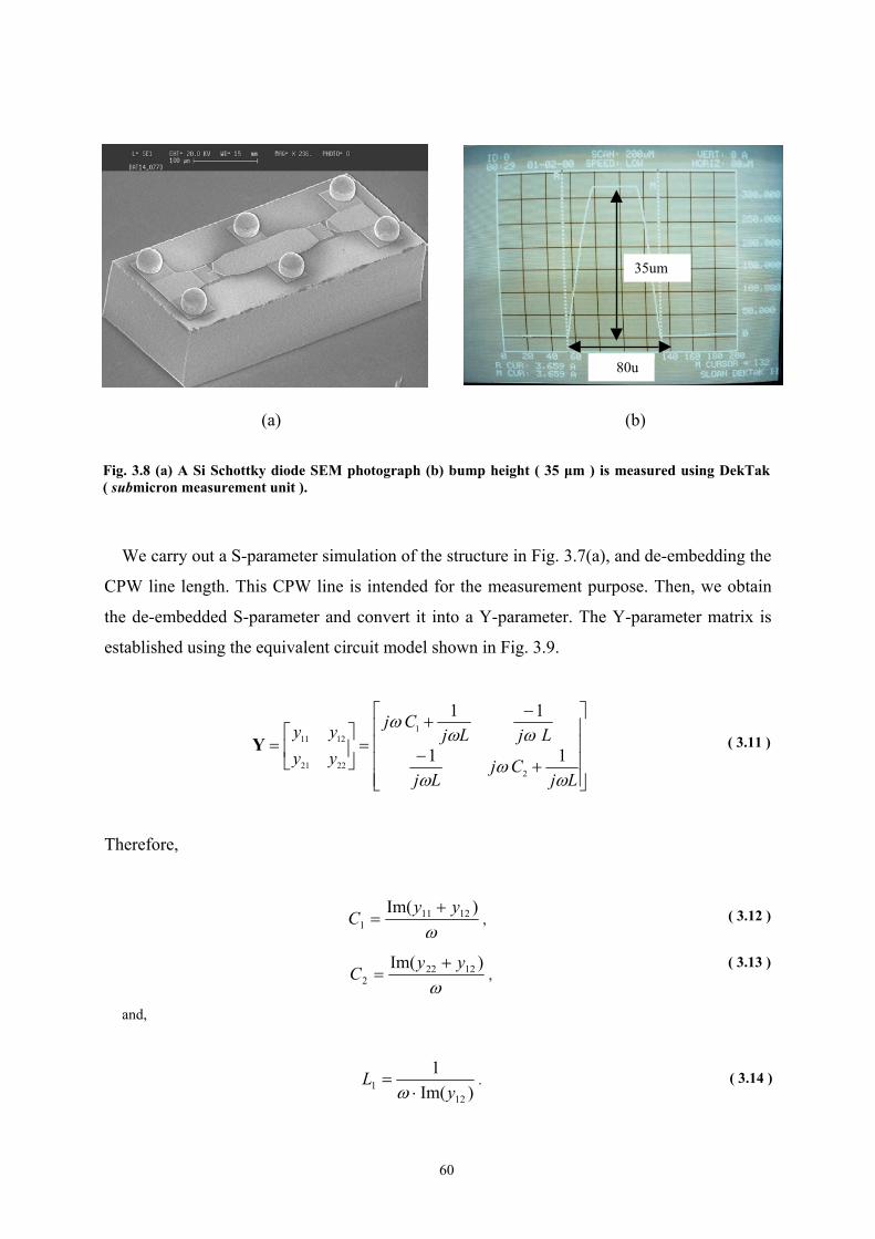
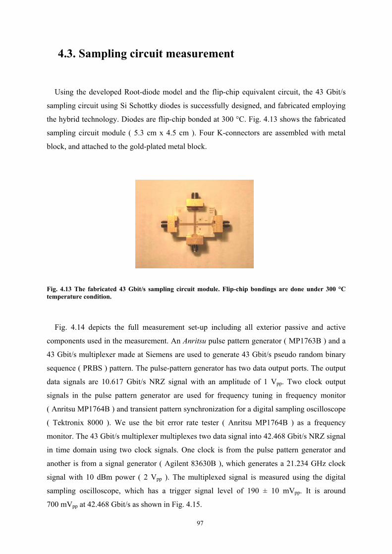
The Si Schottky diode was flip-chip bonded at 300˚C to the backside grounded alumina
substrate, which has a thickness of 250 µm. Bump height after bonding was measured about
5 µm on average. Mechanical bonding force 3.5 N is applied for 5~6 seconds. The used chip
has two Schottky diodes connected in series, and has six pads with one bump each as shown
in Fig. 3.8(a). The chip size is 500 µm x 230 µm, and each bump is made up of AuSn, and
has a height of about 35 µm, as plotted in Fig. 3.8(b). Coplanar waveguides ( CPWs ) with
tapering structures were patterned on the substrate intentionally in order to evaluate the diode
and the flip-chip connection.
Fig. 3.7 (a) A three-dimensional simulation structure in Ansoft HFSS. Si Schottky diode is up-side down, emulating flip-chip bonding structure. (b) Cross sectional view of the flip-chip bonding.
Si Schottky diode
Al2O3 substrate
Alumina substrate ( Al2O3 )
Si Schottky diode
bumpmetallization
C1
C2
Alumina substrate ( Al2O3 )
Si Schottky diode
bumpmetallization
Alumina substrate ( Al2O3 )
Si Schottky diode
bumpmetallization
C1
C2
60
(a) (b)
We carry out a S-parameter simulation of the structure in Fig. 3.7(a), and de-embedding the
CPW line length. This CPW line is intended for the measurement purpose. Then, we obtain
the de-embedded S-parameter and convert it into a Y-parameter. The Y-parameter matrix is
established using the equivalent circuit model shown in Fig. 3.9.
+−
−+
=
=
LjCj
Lj
LjLjCj
yyyy
ωω
ω
ωωω
11
11
2
1
2221
1211Y
Therefore,
ω)Im( 1211
1yyC +
= ,
ω)Im( 1222
2yyC +
= ,
and,
)Im(1
121 y
L⋅
=ω
.
Fig. 3.8 (a) A Si Schottky diode SEM photograph (b) bump height ( 35 µm ) is measured using DekTak ( submicron measurement unit ).
( 3.11 )
( 3.12 )
( 3.13 )
( 3.14 )
80u
35um
61
In Fig. 3.10, simulation results are given varying the simulation frequency from 5 GHz to
40 GHz. As the frequency increases, C2 value gets larger. This phenomenon can be explained
as the overlapping between the dielectric chip and motherboard substrate. However, C1
decreases because this value includes the effect of the bonding pad on the substrate which is
dominant at low frequencies compared to the overlapping effect. Moreover, the summation of
C1 and C2 is almost constant, approximately 90 fF. This means that in the low frequency
region ( e.g. up to 10 GHz ) the overlapping effect ( C2 ) can be neglected compared to C1. As
the frequency increases, these effects are evenly divided showing the similar capacitance
value at 40 GHz.
For a circuit design purpose, the flip-chip bonding simulation results are averaged up to
40 GHz. Those values are summarized in Table. VII.
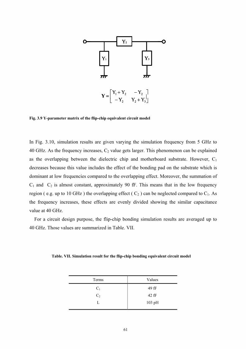
Fig. 3.9 Y-parameter matrix of the flip-chip equivalent circuit model
Table. VII. Simulation result for the flip-chip bonding equivalent circuit model
Terms Values
C1
C2
L
49 fF
42 fF
103 pH
Y1 Y3
Y2
+−
−+=
322
221
YYYYYY
Y
Y1 Y3
Y2
Y1 Y3
Y2
+−
−+=
322
221
YYYYYY
Y
62
(a)
(b)
Fig. 3.10 Flip-chip simulation results for (a) capacitance and (b) inductance varying the frequency until 40 GHz for a bump height of 5 µm.
0 5 10 15 20 25 30 35 40 450
20
40
60
80
100
120
Frequency ( GHz )
Indu
ctan
ce (
pH )
0 5 10 15 20 25 30 35 40 450
10
20
30
40
50
60
70
80
Frequency ( GHz )
Cap
acita
nce
( fF
)capacitance 1capacitance 2
63
3.3. The Root-diode model and the flip-chip simulation verification
Fig. 3.11 illustrates the ADS simulation schematic, in which the Root-diode model is
employed combined with the flip-chip interconnection model. Then conductor-backed
coplanar waveguides ( CPWs ) are added to emulate the feed lines of the test circuit. For
verification purpose, the comparison of measurement with simulation results is performed,
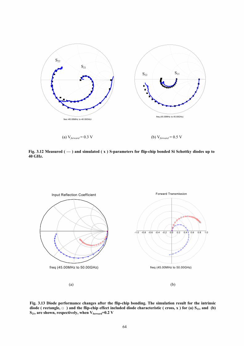
shown in Fig. 3.12. For two forward bias conditions ( 0.3 V, 0.5 V ) we carry out the
simulation. A good agreement between the measured data and the simulation result assures
the exact modeling of the Si Schottky diodes and the flip-chip interconnection up to 40 GHz.
In Fig. 3.13(a) and (b), the S-parameter simulation results are shown with and without flip-
chip interconnection for a diode up to 50 GHz. A forward bias 0.2 V is used for the simulation.
Input reflection coefficient ( S11 ) at 50 GHz shows 5 dB difference in magnitude, and forward
transmission ( S21 ) shows 2.3 dB maximum difference in magnitude at 30 GHz.
Fig. 3.11 The Root-diode model and the flip-chip interconnection model verification. Schematic in ADS simulation environment
Fig. 3.12 Measured ( — ) and simulated ( x ) S-parameters for flip-chip bonded Si Schottky diodes up to 40 GHz.
Fig. 3.13 Diode performance changes after the flip-chip bonding. The simulation result for the intrinsic diode ( rectangle, ) and the flip-chip effect included diode characteristic ( cross, x ) for (a) S11, and (b) S21, are shown, respectively, when Vforward=0.2 V
freq (45.00MHz to 50.00GHz)
Input Reflection Coefficient
-0.8 -0.6 -0.4 -0.2 0.0 0.2 0.4 0.6 0.8-1.0 1.0
freq (45.00MHz to 50.00GHz)
Forward Transmission
65
3.4. Design of the 43 Gbit/s demultiplexer circuit
As discussed in section 2.3, we pursue constructing a high-speed demultiplexer circuit
using the Si Schottky diode instead of transistors. To do that, we need a diode sampling
circuit. The 43 Gbit/s 1:2 demultiplexer circuits are designed and simulated considering both
hybrid and monolithic implementations. First of all, we present sampling circuit design and
simulation results. Then, a tapped delay line filter is examined and designed in the following
section. When the circuit is designed under the hybrid fabrication condition, the flip-chip
equivalent circuit model is attached to each diode pair. Thus, we can acknowledge how the
flip-chip bonding parasitic affects circuit performances compared with the monolithic IC case.
3.4.1. A sampling circuit for the 43 Gbit/s MMIC demultiplexer circuit
3.4.1.1. A sampling circuit schematic and simulation
Fig. 3.14 shows a sampling circuit under the condition of monolithic implementation.
Neglecting the flip-chip bonding connection effect, the intrinsic Root-diode model is
incorporated with the circuit simulator. Three 50 Ω resistances are used in the design: one is
at the input port for matching when the diode pairs are turned off ( non-sampling
instant ). With this resistance, the input signal is completely absorbed, not being reflected
back.
Fig. 3.14 A Si Schottky diode MMIC sampling circuit.
50 Ω
50 Ω
50 Ω CHOLD
Clock
Clock
50 Ω
50 Ω
50 Ω CHOLD
Clock
Clock Clock
66
The other two resistances are for the oscillator signal matching. One capacitor at the output
port of the sampling circuit is to hold the transferred charge from the input port. Series
connected Si Schottky diodes are used in the sampling bridge circuit design. An illustrative
figure of the operation mode is depicted in Fig. 3.15. Four pairs of diodes ( D1, D2, D3, and
D4 ) are aligned in the same direction, forming a signal conducting path from input to output
when the sampling event occurs. One pair of diodes ( D5 and D6 ) counteracts with the others
when the oscillator signals are out of phase compared to the previous state. The oscillation
signals are not reflected back due to this diode pair. A virtual ground is formed in the mid of
D5 and D6 when these two diodes conduct. Thus, to match the oscillator signals, 50 Ω
resistors are connected in series along the oscillator paths.
The diode switching operation is mainly dependent on the external oscillator large-signal.
Once the diodes are turned on, the input signal ( small-signal ) can go through the circuit
toward the output port. Therefore, diode small-signal current can be described by two
components: One is the product of the diode junction voltage with the diode conductance, and
the other is small-signal charge stored in the diode’s junction capacitance [44].
)()()()(DIODE tQdtdttgti j +⋅= υ
( 3.15 )
Fig. 3.15 The simplified operation modes of the bridge circuit. In the left picture, D1, D2, D3, and D4 are conducting (solid line), whereas D5 and D6 are turned off ( dotted line ). In the right picture, vice versa.
D1 D2
D3D4
LOW
HIGH
D5
D6
LOW
HIGH
D1 D2
D3D4
LOW
HIGH
D1 D2
D3D4
LOW
HIGH
D5
D6
LOW
HIGH
D5
D6
LOW
HIGH
67
where, )(tjυ is diode junction voltage, )()()( DIODE tdtidtg jυ= is the diode small-signal
conductance, and )()()( tCttQ j ⋅=υ .
Because the diode capacitance is strongly dependent on the external clock signal rather than
the input signal, it relies on the large-signal, time-varying voltage across the diode’s junction,
and is given by
γ
Φ
−
=
0
0
)(1
)(tV
CtC j
where, 0jC is the zero-voltage junction capacitance, 0Φ is the junction built-in voltage, γ is
the grading coefficient , and )(tV is the time-varying large-signal voltage while )(tjυ in the
equation ( 3.15 ) is small-signal voltage across the p-n junction. Therefore, the small-signal
diode current when the diodes are conducting can be expressed as follows.
)()()()()()()(DIODE tCdtdtt
dtdtCttgti jjj ⋅+⋅+⋅= υυυ
This formula can be interpreted that the diode current comes from three factors: the
contribution of the large-signal excitation of a clock signal, the time-varying small-signal
input, and its time derivative quantity. The transferred charge to the output hold capacitance is
calculated using the following equation,
∫+
⋅=Tk
kT
dttitq)1(
DIODEHOLD )()( .
The instantaneous current and the charge in time domain are simulated using Agilent ADS.
The results are depicted in Fig. 3.16. The output current is calculated using the Kirchhoff
current law at the output port. In Fig. 3.16(a), the negative peaking is obviously shown due to
the two derivative terms in equation ( 3.17 ). When either small-signal voltage across the
diode junction is steeply decreased or the oscillator amplitude decreases, )(tiDIODE shall be
below zero. We also calculated the transferred charge using the current simulation result. The
time period for the calculation was 46.5 psec.
( 3.16 )
( 3.17 )
( 3.18 )
68
(a) (b)
In fact, the small-signal diode current calculation needs both a large-signal and small-signal
analysis in the sampling circuit, because the diode current is also dependent on the time
drivative of the capacitance, which is changed by the large-signal of the oscillator. Analytic
analysis thus needs complicated numerical analysis for our circuit simulation.
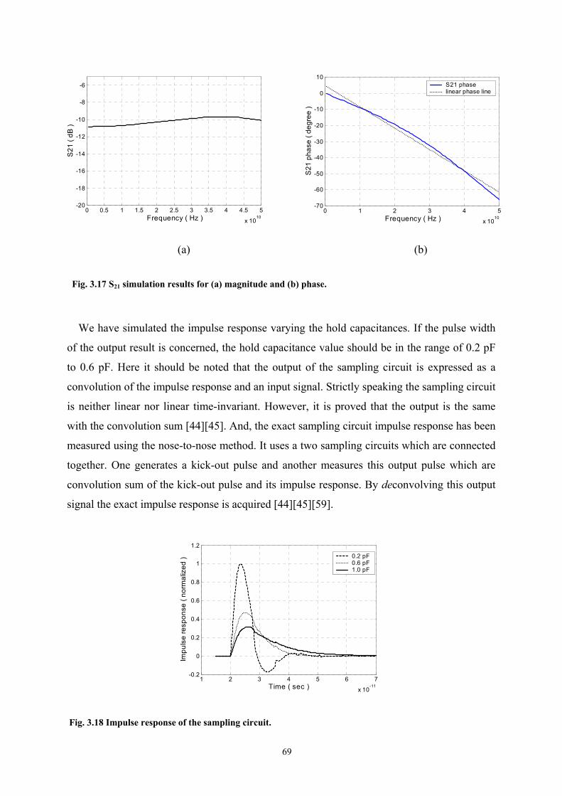
In high-speed digital applications, a linear phase characteristic is of great significance. The
input signal has an ultra broadband frequency spectrum, for example 21.5 GHz fundamental
frequency for 43 Gbit/s NRZ signal. A nonlinear phase response of the system will distort a
signal eye waveform degrading system performance. Thus, we investigate S21 parameter
phase characteristic and also its magnitude response. For simulations, we consider a sampling
instant at which the external oscillator signal is the highest amplitude, and the diode pairs are
fully conducting. The oscillator signal amplitude is set to a constant DC value, 800 mV. The
hold capacitance is 0.2 pF. Even if the fixed oscillator signal amplitude does not emulate the
time-varying sampling actions perfectly, it is still worth while to making use of a simple
situation in order to predict circuit performance at a specific time instant. The same conditions
are used for impulse response simulation in Fig. 3.18. We obtain a very broadband S21
characteristic over 50 GHz. Insertion loss shows 10.2 dB on average until 50 GHz. This is due
to series connected parasitic component of the diode in the current conducting path and
voltage dividing by 50 Ω. In Fig. 3.17(b), a S21 phase simulation result is illustrated with an
interpolated linear phase line. The sampling circuit shows a good linear phase characteristic.
The maximum discrepancy with its linear line is 4.6 ˚ at 500 MHz.
Fig. 3.16 (a) Output current simulation result in the sampling circuit. (b) The transferred charge at the output port is calculated integrating the output current pulses. The charge is normalized and calculated for unity capacitor.
0 0.2 0.4 0.6 0.8 1 1.2 1.4 1.6 1.8 2
x 10-10
-0.4
-0.2
0
0.2
0.4
0.6
0.8
1
1.2
Time ( sec )
Nor
mal
ized
cha
rge
( C )
0 0.2 0.4 0.6 0.8 1 1.2 1.4 1.6 1.8 2
x 10-10
-3
-1
1
3
5
7
x 10-4
Time ( sec )
Cur
rent
( A
)
69
(a) (b)
We have simulated the impulse response varying the hold capacitances. If the pulse width
of the output result is concerned, the hold capacitance value should be in the range of 0.2 pF
to 0.6 pF. Here it should be noted that the output of the sampling circuit is expressed as a
convolution of the impulse response and an input signal. Strictly speaking the sampling circuit
is neither linear nor linear time-invariant. However, it is proved that the output is the same
with the convolution sum [44][45]. And, the exact sampling circuit impulse response has been
measured using the nose-to-nose method. It uses a two sampling circuits which are connected
together. One generates a kick-out pulse and another measures this output pulse which are
convolution sum of the kick-out pulse and its impulse response. By deconvolving this output
signal the exact impulse response is acquired [44][45][59].
Fig. 3.17 S21 simulation results for (a) magnitude and (b) phase.
Fig. 3.18 Impulse response of the sampling circuit.
0 0.5 1 1.5 2 2.5 3 3.5 4 4.5 5
x 1010
-20
-18
-16
-14
-12
-10
-8
-6
Frequency ( Hz )
S21
( dB
)
0 1 2 3 4 5
x 1010
-70
-60
-50
-40
-30
-20
-10
0
10
Frequency ( Hz )
S21
pha
se (
degr
ee )
S21 phase linear phase line
1 2 3 4 5 6 7
x 10-11
-0.2
0
0.2
0.4
0.6
0.8
1
1.2
Time ( sec )
Impu
lse
resp
onse
( no
rmal
ized
) 0.2 pF0.6 pF1.0 pF
70
(a)
(b)
A simulation block diagram for the 43 Gbit/s 1:2 demultiplexer simulation is shown in Fig.
3.19. The ideal 43 Gbit/s pseudo random binary sequence ( PRBS ) of a code length of 27-1 is
generated. Then it is filtered out using a Butterworth low-pass filter, which has a 3 dB
bandwidth of 50 GHz, and the order of 3. The signal is divided into two signals by the
resistive power divider. Due to the 6 dB insertion loss characteristic, each signal amplitude
( 100 mVpp ) is one half of the original signal ( 200 mVpp ). These signals are shown in Fig.
3.20(a) and (b) with their FFT transforms, respectively. The ideal 43 Gbit/s NRZ signal
clearly shows spectral distribution with multiple dips at integer times of 43 GHz. After
filtering, amount of signal power below 43 GHz is still remained, thus the simulated eye
waveform does not show a critical distortion. In general, the power spectral density of the
NRZ signal shows a sinc2 distribution. This fact is obvious from Fig. 3.20(a).
The divided signals are incident on the sampling circuit. The oscillator power for each
sampling circuit is 2 dBm ( ~800 mVpp ). The required oscillator power shall be determined as
the following. The minimum power at least should turn on the diodes while the maximum
power in the diodes should be lower than the thermal breakdown and the reverse breakdown
( 22.5 dBm ).
Fig. 3.19 (a) The 43 Gbit/s PRBS signal ( 200 mVpp) is filtered out using a Butterworth low-pass filter, and divided by the resistive power divider. (b) a 1:2 demultiplexer circuit block diagram using the sampling circuit. After the sampling circuit, the pulse shape filter ( low-pass filter ) is attached.
R
RR
R
RR
fc@ 3dBLow pass filter
PRBS generator
R
RR
R
RR
R
RR
R
RR
R
RR
fc@ 3dBLow pass filter
PRBS generator
R
RR
R
RR
fc@ 3dBLow pass filter
PRBS generator
R
RR
R
RR
R
RR
R
RR
R
RR
fc@ 3dBLow pass filter
PRBS generator
t = kTS
Diode sampler
t = kTS
Diode sampler
t = (k+1)TSDiode samplert = (k+1)TS
Diode sampler
R
RR
R
RR
R
RR
R
RR
R
RR
fc@ 3dBLow pass filter
PRBS generator
R
RR
R
RR
R
RR
R
RR
R
RR
R
RR
fc@ 3dBLow pass filter
PRBS generator
t = kTS
Diode sampler
t = kTS
Diode sampler
t = (k+1)TSDiode samplert = (k+1)TS
Diode sampler
71
(a)
(b)
A pulse shaping low-pass filter ( Bessel-Thompson filter having a bandwidth of 10.75 GHz
and the order of 5 ) is added to obtain the demultiplexed signal waveform. In addition, we
employ one commercial amplifier to increase signal amplitude [52]. The amplifier has a gain
of 15 dB up to 42 GHz. The measured S-parameters for the amplifier is added to the circuit
schematic for the demultiplexer circuit simulation. The delay of the oscillator signal is tuned
observing the output eye waveform. The simulated output waveforms for two channels are
shown in Fig. 3.21. We use a hold capacitance of 0.2 pF at the output of the sampling circuit.
Compared with Fig. 2.11, which is an ideal demultiplexed waveform, the simulation results
using the actual diode model show a good agreement. The waveform is still NRZ-like
waveform. However, we note that the eye waveform is distorted due to the intersymbol
interference. This is caused by the pattern dependent deterministic behavior of the circuit.
Furthermore, the distorted bit and the adjacent bit differ from the channel number. Therefore,
we shall model these distorted channel results as two coupled channels. Each channel
generates a crosstalk depending on the bit pattern. The amount of crosstalk quantity will be
calculated using the aforementioned zero-forcing algorithm.
Fig. 3.20 (a) Ideal 43 Gbit/s eye diagram, and its FFT result. 43 Gbit/s NRZ signal has a period of fundamental frequency component of signal, 43 GHz. (b) Filtered 43 Gbit/s NRZ signal. High frequency component is considerably reduced.
0 10 20 30 40 50 60 70-10 80
0.05
0.10
0.15
0.00
0.20
Time ( psec )
Am
plitu
de (
V )
20 40 60 80 100 120 140 160 1800 200
-150
-100
-50
-200
0
Frequency ( GHz )
Mag
nitu
de (
dB
)0 10 20 30 40 50 60 70-10 80
-0.00
0.02
0.04
0.06
0.08
0.10
-0.02
0.12
Time ( psec )
Am
plitu
de (
V )
20 40 60 80 100 120 140 160 1800 200
-120
-100
-80
-60
-40
-140
-20
Frequency ( GHz )
Mag
nitu
de (
dB
)
72
(a)
(b)
Fig. 3.21 Eye diagrams of demultiplexed (a) channel 1 and (b) 2, respectively. ( CHOLD=0.2 pF )
0 20 40 60 80 100 120-20 140
0.00
0.02
0.04
0.06
-0.02
0.08
Time ( psec )
Am
plitu
de (
V )
0 20 40 60 80 100 120-20 140
0.00
0.02
0.04
0.06
-0.02
0.08
Time ( psec )
Am
plitu
de (
V )
73
3.4.2. The transversal tapped delay line filter
A tapped delay line filter is designed for the purpose of reducing the ISI phenomenon. We
consider that the finite number of symbols, 2M+1, will affect the ISI. Thus, the kth output
symbol, kouts ,ˆ , is a function of 2M+1 elements given by
∑
∑
≠−=
+
−=+
+−+++−−
+=
=
=
M
jMj
jkjk
M
Mjjkj
MkMkkkMkMkkout
spsp
sp
ssssssfs
0
0
1,11, ),,,,,,(ˆ KK
where, using equation ( 2.76 ) kp is expressed as,
∑−=
−=⋅=L
Liikkik hgp ,k
Hk hG .
The condition to satisfy the zero-forcing algorithm can be alternatively described using
parameter kp given by,
=
=otherwise0
0if1 kpk .
Here we use the normalized parameter kp . In order to apply this algorithm to the transversal
equalizer circuit design, we consider the simple case for M=1. It means that the output is
assumed to be affected by one past and one future bit.
11,ˆ +− ⋅++⋅= kkkkout ssss βα
Expressing the above equation in z-domain, the transfer function is given by
( 3.19 )
( 3.20 )
( 3.21 )
( 3.22 )
74
zzzH ⋅++⋅= − βα 1)( 1
Applying ( 3.23 ) into ( 3.20 ), we obtain the transversal tapped delay line filter coefficients as,
.21
and,211,
21 101 αβα
αβαββ
−−
=−
=−−
=− ggg
Therefore, we can conclude that the equalizer transfer function is written by,
( )11211)( −⋅−+⋅−
−= zzzHEQ αβ
αβ
Comparing the equalizer transfer function with Fig. 3.22, and assuming the symmetry
between two channels, the coefficients can be chosen as,
ααβαβ
αββ
−≈−−
==−≈−−
==21
and,21 1100 DCDC .
( 3.23 )
( 3.24 )
( 3.25 )
( 3.26 )
Fig. 3.22 Proposed transversal filter to equalize ISI phenomena.
Z-2
C0 C1
Σ
Z-2
D0D1
Σ
Z-1 Z-1
Ch.1 Ch.2
Ch.1 Ch.2
Z-2
C0 C1
Σ
Z-2
D0D1
Σ
Z-1 Z-1Z-1
Ch.1 Ch.2
Ch.1 Ch.2
75
In determining the coefficients α and β , first of all the ISI quantity should be considered.
We employ (······0001000······) symbols to see how much ISI affect the adjacent bit. A single
‘1’ bit is applied to a sampling circuit for channel 1, then we observe the ISI-affected
waveform of the adjacent bits in channel 2. The following equation is used to decide the
coefficients,
MAX
s
TtLPFChsampler
K
KmmTtLPFChsampler
ISI
thtS
thtS
=
−==
=∑
)(*)(max
)(*)(max
1.
2.ρ
where K represents the number of significance bits, Ts is an optimum sampling instant for
channel 2, and Tmax is for channel 1. By circuit simulation, we find out the coefficients.
)dB56.15(167.0 −== βα . A simulation result is given in Fig. 3.23.
(a)
(b)
( 3.27 )
Fig. 3.23 Eye waveform (a) before equalization, and (b) after equalization
0 20 40 60 80 100 120-20 140
0.00
0.02
0.04
0.06
-0.02
0.08
Time ( psec )
Am
plitu
de (
V )
0 20 40 60 80 100 120-20 140
0.00
0.02
0.04
0.06
-0.02
0.08
Time ( psec )
Am
plitu
de (
V )
76
To evaluate the equalizer circuit performance we calculate eye opening using the following
equation [55],
(%)100)0ˆ(max)1ˆ(min
opening Eye,,
⋅=−=
=Y
ssss koutkkkoutkk
where Y means the ISI free case. In Table. VIII, the eye opening calculation is summarized.
before equalization after equalization
Eye opening ( % ) 45.3 % 57.6 %
It is noted that the adaptive signal processing to track the impairments from the imperfect
receiver response is preferred to enhance the signal integrity. However, recognizing the
operability of commercial devices up to multi gigabit-per second data rates ( for instance,
power amplifier, power divider, delay lines, and filters ), the constraint exists in case of
80 Gbit/s and 160 Gbit/s for equalizer realization. So far, electronic equalization has been
reported in [53]-[57] using adaptive and non-adaptive ways, which include linear, non-linear
and maximum-likelihood methods. Even though the proposed transversal filter equalization
method is adaptable to many types of distortion, this technique has also disadvantages [57].
Among them, one peculiar characteristic of this type equalizer is the amplification of the
noise at specific frequency, therefore it requires many taps to compensate. The other is the
disability for non-linear distortions.
( 3.28 )
Table. VIII Eye opening calculation before and after equalization.
77
3.4.3. 43 Gbit/s hybrid demultiplexer circuit
A hybrid sampling circuit is designed considering the flip-chip bonding technology. The
flip-chip equivalent circuit in Fig. 3.6 is applied to the circuit design. An alumina substrate
and the conductor-backed coplanar waveguide ( CPW ) with via holes are also employed. The
circuit schematic is fundamentally the same as in Fig. 3.14. We investigate the circuit
performance comparing with the MMIC circuit simulation results. Also, the tapped delay line
filter simulation is carried out. First of all, Fig. 3.24 shows impulse responses of the hybrid
sampling circuit for various hold capacitors.
The simulation condition is the same with that of the MMIC sampling circuit. It is obvious from Fig. 3.24 that
flip-chip parasitics change its intrinsic impulse response considerably. Rise and fall time increase in the hybrid
circuit, and a trailing edge is more irregularly oscillating and seldomly die out completely as simulation
sweeping time increases. The full width at half maximum ( FWHM ) value is measured. It increases from 6 psec
to 18 psec in the hybrid circuit when the hold capacitance is 0.2 pF. The S21 parameter simulation results are
shown in Fig. 3.25. They are compared with MMIC circuit simulation results. The simulated 3 dB cutoff
frequency is 26 GHz while in the MMIC circuit above 50 GHz cutoff freqeucny is estimated. The phase changes
more rapidly in the hybrid circuit. Above 43 GHz the nonlinear phase characteristic starts to show up. We
investigate the group delay characteristic. Until 37 GHz, it deviates ±13 psec from the average value, 31.5 psec.
Around 50 GHz spectral components begin to be lagged down.
Fig. 3.24 Impulse response simulation results including flip-chip parasitics for various hold capacitances.
0 0.1 0.2 0.3 0.4 0.5 0.6 0.7 0.8 0.9 1 1.1
x 10-10
-0.4
-0.2
0
0.2
0.4
0.6
0.8
1
1.2
Time ( sec )
Impu
lse
resp
onse
( no
rmal
ized
) 0.2 pF0.6 pF1.0 pF
78
(a) (b)
The hybrid sampling circuit simulations for the demultiplexer are done with the equalizer.
Their results are given in Fig. 3.27. Simulation conditions are all the same with the MMIC
case. The hold capacitance value is 0.2 pF, and the equalizer coefficients are 15 dB. In
contrast to the MMIC circuit simulation results, the equalizer enhances the eye opening by
5 %.
Fig. 3.25 S21 of the hybrid circuit is compared with those of the MMIC sampling circuit for (a) magnitude and (b) phase.
Fig. 3.26 Group delay of the hybrid sampling circuit.
0 1 2 3 4 5
x 1010
-50
-45
-40
-35
-30
-25
-20
-15
-10
-5
Frequency ( Hz )
S21
( dB
)
MMIC samplerHybrid sampler
0 1 2 3 4 5
x 1010
-200
-150
-100
-50
0
50
100
150
200
Frequency ( Hz )
S21
pha
se( d
egre
e )
MMIC samplerHybrid sampler
0 1 2 3 4 5
x 1010
-6
-4
-2
0
2
4
6
8x 10
-11
Frequency ( Hz )
Gro
up d
elay
( se
c )
79
(a)
(b)
This small enhancement can be explained with regard to the irregular trailing edge in the
impulse response. The edge affects several adjacent bits, thus the equalizer circuit needs more
than three taps. And, it is sophisticated to determine the filter coefficients because the ISI
depends on both bit patterns and the irregular trailing edges by each pattern. So, we use the
averaged coefficient value for the equalizer circuit simulation. Those constant should be
verified with the experimental result. It is noted that the output amplitude is reduced by half
compared with the MMIC simulation result. The main loss comes from the flip-chip parasitics.
For the equalizer in the hybrid sampling circuit, the adaptive algorithm is another choice to
consider. Keeping track of the eye waveform variation, the filter coefficients can be
adaptively changed and the clean eye waveform is obtained. However, the complexity of the
receiver structure and the high-speed adaptive signal processor implementations are also
considered.
Fig. 3.27 The hybrid circuit simulation result (a) before and (b) after equalization
0 20 40 60 80 100 120 140-20 160
0.00
0.01
0.02
0.03
-0.01
0.04
Time ( psec )
Am
plitu
de (
V )
0 20 40 60 80 100 120 140-20 160
0.00
0.01
0.02
0.03
-0.01
0.04
Time ( psec )
Am
plitu
de (
V )
80
3.5. 86 Gbit/s MMIC 1:2 demultiplexer circuit
3.5.1. 86 Gbit/s MMIC 1:2 demultiplexer
In this section we show that the sampling concept using Si Schottky diodes for the
demultiplexer circuit is feasible for an 86 Gbit/s 1:2 demultiplexer or higher speed circuit
implementation. We propose a circuit schematic and present simulation results for
an 86 Gbit/s demultiplexer. It is of significance to show that the Si Schottky diode sampling
circuit would be expanded into a higher bit rate communication circuit. Circuit simulation
results are provided supporting this fact. A linear equalizer circuit is also utilized to obtain a
demultiplexed signal waveform. As discussed in chapter 1, this work is motivated by the fact
that high-speed digital circuits can be implemented by analog ways using Si Schottky diodes.
Challenging to the 86 Gbit/s demultiplexer circuit, we present the Si Schottky diode sampling
circuit based demultiplexer circuit and simulation results.
3.5.1.1. Operation principle and simulation results
The circuit topology is different from the 43 Gbit/s 1:2 demultiplexer circuit. In order to
achieve higher bit rate using Si Schottky diodes, the structure itself is minimized. The same
diode model in the previous section is used for 86 Gbit/s MMIC 1:2 demultiplexer circuit
simulation.
Eliminating the requirement of the broadband resistive power divider, an integrated 1:2
demultiplexer is developed ( see Fig. 3.28 ). It is composed of two sampling circuits. Both of
them are equivalent and connected in parallel sharing the same oscillator signal. The distinct
difference is the direction of the diode pair. The diodes are anti-parallel, but each sampling
circuit is fundamentally identical. Compared with the sampling circuit for the 43 Gbit/s 1:2
demultiplexer, a 50 Ω matching resistance is removed and the number of used diodes is
smaller than that of the 43 Gbit/s sampling circuit. It is also beneficial to use the decreased
number of oscillator signal, because we do not need to supply high power oscillating signal
for the switching operation. The illustrative figure is illustrated in Fig. 3.28. Depending on the
clock signal amplitude, diode pairs are either conducting or not. Because diode pairs are anti-
81
CHOLD
CHOLD
Input
''1''
''0''
D1
D2
D3
D4
CHOLD
CHOLD
Input
''1''
''0''
D1
D2
D3
D4
CHOLD
CHOLD
Input
''1''
''0''
D1
D2
D3
D4
CHOLD
CHOLD
Input
''1''
''0''
CHOLD
CHOLD
Input
''1''''1''
''0''''0''
D1
D2
D3
D4
(a) (b)
parallel each other, one diode pair flows current during the other remains off-state, and vice
versa. Thus, in either case, the input signal can find the path to flow toward one of the output
ports. In this way, the resistive power divider can be removed. When analyzing the circuit
operation, time-domain method is performed to characterize time-dependent impedance and
current. Small-signal bandwidth analysis also is carried out, and they are presented in [63][64].
The eye diagram simulation results are shown in Fig. 3.29. The hold capacitance is 0.2 pF and
oscillator signal power is 0.88 dBm ( 700mVpp ).
(a) (b)
Fig. 3.28 An 86 Gbit/s demultiplexer circuit operation principle is illustrated when (a) only D1, and D2 diodes are conducting, and (b) only D3, and D4 are conducting. In each case, their clock signal amplitude is presented.
Fig. 3.29 The 86 Gbit/s MMIC 1:2 demultiplexer circuit simulation results using Si Schottky diode sampling circuit. Demultiplexer circuit output signals are presented (a) before and (b) after equalization
0 10 20 30 40 50 60 70-10 80
0.000
0.005
0.010
0.015
0.020
-0.005
0.025
Time ( psec )
Am
plit
ude
( V
)
0 10 20 30 40 50 60 70-10 80
0.000
0.005
0.010
0.015
-0.005
0.020
Time ( psec )
Am
plit
ud
e (
V )
82
At the end of the output port, a low-pass filter ( Bessel filter of order 5 and bandwidth
of 21.5 GHz ) is connected to form a 43 Gbit/s NRZ waveform. In 86 Gbit/s optical receiver
application, we use 86 Gbit/s RZ signal as an input signal to the sampling circuit and generate
the signal using the 5th order Bessel filter having a bandwidth of 55 GHz. The filtered signal
has a peak amplitude of 200 mVp. The ideal signal and the filtered RZ signal are shown in Fig.
3.30. As shown in Fig. 3.30(b) and (d), the 86 Gbit/s RZ signal has a spectral peak at odd
multiples of 86 GHz, i.e., 86 GHz, 258 GHz. The spectral peak at 86 GHz shall be used to
synchronize the data stream with the clock signal in phase-locked loop ( PLL ) circuit. The
circuit output signal is post processed with a linear tapped delay line filter, which is explained
in section 3.4.2. We find out the filter coefficients using equation ( 3.27 ). The constants,
C0=D0=C1=D1= -10 dB, are calculated in the same way as discussed in section 3.4.2. We use
equation ( 3.28 ) to get eye opening parameter. It is obvious that the eye opening is improved
considerably from 33.3 % to 58.3 %. Therefore, we are in success to show that the 86 Gbit/s
demultiplexer circuit is feasible using Si Schottky based sampling circuit.
(a) (b)
(c) (d)
Fig. 3.30 (a) Ideal 86 Gbit/s RZ signal eye diagram, and its FFT result. (b) Filtered 86 Gbit/s RZ signal.
83
4.1. Coplanar waveguide measurement and analysis
The hybrid technology is employed to fabricate the designed sampling circuit. To do so,
first of all, conductor-backed coplanar waveguides ( CPWs ) with via holes are designed and
fabricated using the alumina substrate with 10 mil ( 254 µm ) thickness. The significant
electrical parameters of the substrate to consider are summarized in Table. IX.
First of all, in high-speed digital circuit applications the substrate thickness should be
decided carefully. As the substrate thickness increases with constant W/S ratio ( Fig. 4.1(b) ),
the higher-mode cutoff frequency decreases. When the cutoff frequency is inside the spectral
region of interest, the digital signal waveform suffers from distortion. In a conductor-backed
dielectric slab waveguide, the first higher mode ( TE1 mode ) cutoff frequency is inversely
proportional to dielectric thickness, and it is given by
141 −=
rTE h
cfε
where h means the substrate thickness, c is the light velocity, and rε is the relative dielectric
constant of the substrate. Thus, the substrate thickness, W, and S should be chosen in order to
increase the cutoff frequency of the first higher mode of the slab waveguide and of the CPW.
where ),( zfV is the Fourier transform of ),( ztυ , )( fα is the frequency dependent
attenuation coefficient, and )( fβ is the frequency dependent phase. ( )⋅−1F denotes an
inverse Fourier transformation.
The CPW loss is composed of dielectric loss, conductor loss, and radiation loss. Usually,
the dielectric loss is much smaller than the conductor loss and negligible [72]. If no leaky
wave mode is excited, the conductor loss is dominant source for the attenuation. However,
above 200 GHz the radiation loss starts to be dominant [70]. The radiation leakage occurs
because of surface waves in the conductor-backed slab waveguide. Therefore, the attenuation
coefficients can expressed as the summation of conductor loss and radiation loss by
radcond ααα += .
The dispersion problem arises from the frequency-dependent characteristics of the
propagation constant associated with physical geometries of the structures, i.e., coplanar
waveguides or microstrip lines. The frequency-dependent nature of the signal propagation
constants causes signal distortion, in other words, the propagated signal shows the pulse
broadening effect. The dispersion characteristic is modeled using the following equation.
effcff επβ 2)( =
where effε is the effective dielectric constant and analytic equation is shown below.
( 4.4 )
( 4.5 )
( 4.6 )
88
⋅+
−+=
− 8.1
1
1
1
)(
TE
qrq
neff
ffa
fεε
εε
where, 2
1+= r
qεε , rε is the relative dielectric constant of the substrate, n is 2, fTE1 is given
in ( 4.1 ), and a is found using [70],
( )
2
2
log540.0log86.043.0
log015.0log69.054.0
loglog
⋅+
⋅−=
⋅+
⋅−=
+
⋅=
hW
hW
hW
hWu
SWua
υ
υ
where h is the thickness of the substrate. The calculation for the attenuation and the effective
dielectric constant are carried out using the measured S-parameter. The S-parameter response
of the lossy unmatched transmission line is expressed as [73][74],
−−
=
lZZZZ
ZZlZZDSS
SS
oo
oo
s γγ
sinh)(22sinh)(1
22
22
2221
1211
where, lZZlZZD oos γγ cosh2sinh)( 22 ++= . Using the equation ( 4.9 ), the following
equation can be derived directly,
( )( )2
21
221
2221
211
21
221
211
241
21
SSSS
SSSe l −−−
±+−
=−γ
where ( ) ( ) )()()( fjfCjGLjRf βαωωγ +=+⋅+= , and we use the symmetry condition
for port 1 and port 2, namely, 2211 SS = , and 2112 SS = . The positive sign is used to find the
negative direction propagation constant, and the negative sign is for the positive direction.
( 4.7 )
( 4.8 )
( 4.9 )
( 4.10 )
89
(a) (b)
The extraction results are shown in Fig. 4.4. The attenuation coefficient is normalized with
regard to the length. The length of the CPW we designed is 20 mm. Effective dielectric
constant is also extracted and compared with the analytic calculation in ( 4.7 ). We change the
coefficient n into 1.9 in order to fit the extracted data. In fact, the analytic expression is
derived for the conductor-backed CPW without via holes. Therefore, the n value difference is
attributed to the discrepancies of the propagation characteristics with via holes. We also
investigate the group delay characteristic. The group delay is defined as,
dffd
fT)(
21
)(Φ
−=π
.
where )( fΦ is the phase response of the CPW. The group delay is calculated using the
measured S21 parameter. We compared the extracted result with the interpolation result as
shown in Fig. 4.5. The interpolation is done for the frequency band from 3 GHz to 50 GHz
with couples of points. It shows a constant group delay until 23 GHz. At 43 GHz the group
velocity deviates from the constant delay line about 6.1 psec. We characterize this relation
ship with the following equation,
Fig. 4.4 (a) Measured attenuation constant and (b) Comparison of the measured with the calculated effective dielectric constant, respectively.
( 4.11 )
0 1 2 3 4 5
x 1010
1
2
3
4
5
6
7
8
9
10
11x 10
-3
Frequency ( Hz )
Atte
nuat
ion
( Np/
mm
)
0 1 2 3 4 5
x 1010
3
3.5
4
4.5
5
5.5
6
6.5
7
7.5
8
Frequency ( Hz )
Effe
ctiv
e di
elec
tric
cons
tant
MeasurementCalculation
90
⋅+⋅⋅≈
⋅⋅=Φ
0102
)(2)(
ffTTf
fTff
π
π
where for 43 Gbit/s NRZ signal, GHz430 =f , 0T is constant value, 460 psec for 20 mm
length of the conductor-backed CPW with via holes, and 1T is 6.1 psec.
Using the above results, i.e., the attenuation coefficient, and the dispersion parameter, we
simulate how both of them change the eye waveform for the different propagation lengths.
The eye waveform depicts the signal waveforms by overlapping them in limited time window.
It clearly shows the signal waveform at specific distance. In Fig. 4.6(a) the input signal to the
designed conductor-backed CPW line is shown. This is equivalent to the Fig. 3.20(b). For 4
cm and 8 cm long length, the simulation results are presented in Fig. 4.6(a) and (b),
respectively. As the propagation is increased, the distortion and the signal amplitude
attenuation are clearly shown.
Fig. 4.5 Group delay is extracted from the S21 parameter ( solid line ). Interpolation line is performed for the measurement results ( dotted line).
( 4.12 )
1.0E10 2.0E10 3.0E10 4.0E100.0 5.0E10
460
465
470
455
475
Frequency ( Hz )
Gro
up d
elay
( p
sec
)
91
(a)
(b)
(c)
Fig. 4.6 (a) Eye diagram of the 43 Gbit/s at the input after 5th order Bessel filter. Eye opening are observed for (b) 4cm and (c) 8cm long conductor-backed CPW lines
0 10 20 30 40 50 60 70-10 80
0.00
0.05
0.10
0.15
0.20
-0.05
0.25
time, psec
vin_
eye
0 10 20 30 40 50 60 70-10 80
0.00
0.05
0.10
0.15
0.20
-0.05
0.25
time, psec
vout
_eye
0 10 20 30 40 50 60 70-10 80
0.00
0.05
0.10
0.15
0.20
-0.05
0.25
time, psec
vout
_eye
92
4.2. Resistive power divider circuit design and measurement
A resistive power divider divides an input signal into two having a 6 dB insertion loss.
Therefore, the divided signal amplitude is halved. Once each port is terminated with 0Z
( 50 Ω ) in Fig. 4.7(a), the input impedance shows a matched condition written by,
0000
34||
34
3ZZZZZin =+=
If the input voltage to the input is V, then the output voltage at port 2 and 3 is found as,
VZZ
ZZZ
ZVVout 21
332332
00
0
00
0 =+
⋅+
⋅= .
If this network is symmetric, then the 3 port S-parameter matrix is given by
Substituting [ A.4 ] with [ A.5 ] and [ A.9 ], we finally acquire the expression for the
autocovariance of the photocurrent.
( )
( )
∫ ∫
∫ ∫
∫ ∫
∞
∞−
∞
∞−
∞
∞−
∞
∞−
∞
∞−
∞
∞−
∆
⋅−−⋅+
⋅−−ℜ⋅+
⋅+⋅=
−−+=
−=∆⋅∆=
')'()()'()(
')'()()'()()'()(2
))(*())(*)((
')'()()',()(*)(
)'()()'()()'()(',
2*2
*2
22
222
ττττττ
ττττττττ
ττττττ
ddththR
ddththOOR
thPqRthtpqR
ddththCRthtR
titititititittC
PDPD
PDPDSIGSIG
PDNPDSIG
PDPDPD
i
NN
NN
ORX
OO
OO
ORX
[ A.7 ]
[ A.8 ]
[ A.9 ]
[ A.10 ]
107
Appendix B
Si Schottky diode demultiplexer circuit MATLAB program
%--------------------------------------------------------------------% % Author : Jung Han Choi % Parameter definitions %--------------------------------------------------------------------% % Nyquist wavefrom Roll-off factor. Ref : IEEE Journal of Light. Tech. Vol.19, No. 9, pp. 1263-1273, Sep. 2001. alpha=0.4; % td : pulse width % 40 Gbps NRZ : td=25.00e-12 sec, 80 Gbps RZ : td= 6.25e-12 sec td=6.25e-12; % Number of periods in the Nyquist waveform num_period=1; % Number of points in one period of waveform pts=100 ; %--------------------------------------------------------------------% % Simulation range definition in time domain. % start and stop points should be integer times of period % e.g.) start_time=0,stop_time=100 means that simulation time is % from 0(sec) to 100*td ( sec ) ( 0 ~ 100T ) for NRZ signal % from 0(sec) to 100*td*2 ( sec ) ( 0 ~ 100T ) for RZ signal %--------------------------------------------------------------------% start_time=0; stop_time=30; %--------------------------------------------------------------------% % Random input signal generation combining with Nyquist waveform and pseudo-random binary sequence ( PRBS ) %--------------------------------------------------------------------% e=[]; e=input_signal(td, alpha, pts, num_period, start_time, stop_time); %--------------------------------------------------------------------% % 5th order Bessel-Thompson filter . Input_signal passes through the filter. We depict eye diagram after the filter. %--------------------------------------------------------------------% num=[0 0 0 0 0 945]; den=[1 15 105 420 945 945]; [A B C D]=tf2ss(num,den); % Converts into the state-sapce domain [G H]=c2d(A, B, 0.01375); % 55GHz / 8000GHz ( 80G NRZ ) *2 % 8000GHz : sampling frequency. One period of 80 Gbit/s RZ signal ( 2*6.25psec ) is subdivided by 'pts'. % Thus,sampling time difference is 2*6.25psec / 100 pts, which corresponds to 8000 GHz. [numz denz]=ss2tf(G,H,C,D); y=filter(numz, denz, e); eye_waveform(y, td, pts, 0); % Draw eye diagram
108
%--------------------------------------------------------------------% % Sampling process ( demultiplexing ) %--------------------------------------------------------------------% figure;x=start_time:1/pts:stop_time; subplot(5,1,1); plot(x,y); % Plot PRBS Nyquist waveform after Bessel filter subplot(5,1,2); % Generate impulse train for channel 1 and draw it imp_sampler_ch1=transfer_sampler(2*td, 2*pts, start_time, stop_time, 6.25e-12); % Perform sampling ( demultiplexing ) for channel 1 output_sampling_ch1=sampling(y, imp_sampler_ch1); subplot(5,1,3); % Generate impulse train for channel 2 and draw it imp_sampler_ch2=transfer_sampler(2*td, 2*pts, start_time, stop_time, 12.5e-12); % Perform sampling ( demultiplexing ) for channel 1 output_sampling_ch2=sampling(y, imp_sampler_ch2); % Depict the sampled waveform in time domain for channel 1 and 2 subplot(5,1,4); plot(x,output_sampling_ch1); subplot(5,1,5); plot(x,output_sampling_ch2); %--------------------------------------------------------------------% % The sampled signal passes through a low-pass filter ( LPF ) to make its demultiplexed waveform. %--------------------------------------------------------------------% [G H]=c2d(A, B, 0.005); % 20 GHz /8000GHz ( 40G NRZ ) *2 [numz denz]=ss2tf(G,H,C,D); % Sampled signal ( channel 1 ) is filter out by the 5th order Bessel filter % which has a bandwidth of 20GHz. yy=filter(numz, denz, output_sampling_ch1'); % Draw eye diagram eye_waveform(yy, td, pts, 0); ------------------------------------------------------SUBROUTINE 1------------------------------------------------------ %--------------------------------------------------------------------% % Signal modeling % Function usage : input_signal(td, alpha, pts, num_period, start_time, stop_time) % % This function generates PRBS waveform in time domain. % The pulse used here is Nyquist waveform with roll-off factor, 0<alpha<1. % % 1. Pulse width : td % 2. Nyquist coefficient : alpha % 3. # of points in one pulse duration : pts % 4. # of periods in Nyquist waveform : num_period % 5. start time point : start_time % 6. stop time : stop_time %--------------------------------------------------------------------% function e=input_signal(td, alpha, pts, num_period, start_time, stop_time) % Nyquist waveform generation with Roll-off factor and pts. pulse=Nyquist_pulse(alpha,pts,num_period); % PRBS sequence 2^8-1 generation (Subroutine PRBS_seq) PRBS_sequence=PRBS_seq(8); % input signal matrix initialization e([1:(stop_time)*pts+1],:)=0;
109
% 80 Gbps RZ case for i=start_time:stop_time+num_period-1, if(-i<-num_period) p_start=-num_period; else p_start=-i; end; if(i+num_period)>stop_time p_stop=stop_time-i; else p_stop=num_period;end; temp_pulse=pulse([(p_start+num_period)*pts+1:(p_stop+num_period)*pts+1],:); if(i<=num_period) index=0; else index=i-num_period;end; temp_index=0; for k=index*pts+1:index*pts+size(temp_pulse,1), temp_index=temp_index+1; e(k,:)=e(k,:)+temp_pulse(temp_index)*PRBS_sequence(i+1); end end ------------------------------------------------------SUBROUTINE 2------------------------------------------------------ %--------------------------------------------------------------------% % PRBS (Pseudo-random Binary Sequence) generator Program % PRBS(num_stage) % PRBS() generate PN sequences with user-defined recurrence relation. % num_register ; # of shift register in Linear Feedback Shift Register(LFSR) % Note that Student version of MATLAB supports not more than 14 shift registers. %--------------------------------------------------------------------% function p=PRBS_seq(num_register) if (num_register<2|num_register>33) error('Num_register represents the number of shift register in Linear Feedback Shift Register'); error('num_register should be larger than 2, or smaller than 33 in this version'); end % Tap reference ref_tap=[2 1 0 0;3 1 0 0;4 1 0 0;5 2 0 0;6 1 0 0;7 1 0 0;8 4 3 2;9 4 0 0;10 3 0 0;11 1 0 0;12 6 4 1; 13 4 3 1;14 12 2 1;15 13 10 9;16 12 3 1;17 3 0 0;18 7 0 0;19 5 2 1;20 3 0 0;21 2 0 0;22 1 0 0; 23 5 0 0;24 7 2 0;25 3 0 0;26 6 2 1;27 5 2 1;28 3 0 0;29 2 0 0;30 23 2 1;31 29 21 17;32 22 2 1; 33 13 0 0]; tap=ref_tap(num_register-1,:); temp=0; for i=1:size(tap,2), if tap(i)>0, temp=temp+1; end; end; size_tap=temp; num_stage=max(tap); % Seed is assumed to be '1'. state(1:num_stage)=1; p=[];p_final=[]; for index=1:2^num_stage-1, tot=0; for sub=1:size_tap,tot=XOR(tot,state(tap(sub))); end; state(1:num_stage)=[tot,state(1:num_stage-1)]; p=[p;state(num_stage)]; end return ------------------------------------------------------SUBROUTINE 3------------------------------------------------------ %--------------------------------------------------------------------% % Nyquist pulse generation and plotting % function usage ; Nyquist_pulse(alpha,pts, num_period); % Nyquist Roll-off factor : alpha % Number of points in one period : pts % # of periods to calculate : -num_period*T ~ num_period*T
110
%--------------------------------------------------------------------% function pulse=Nyquist_pulse(alpha, pts, num_period) x=[];pulse=[];temp=[]; % Ref. IEEE journal of Light. Tech. Vol. 19, No. 9, pp.1263-1273, Sept. 2001. % d_cycle means duty cycle of Return-to-Zero signal. % If d_cycle is equal to '1', then the waveform becomes Nonreturn-to-Zero. d_cycle=0.33; for x=-num_period:1/pts:num_period, if alpha*d_cycle<x & x< d_cycle pulse=[pulse,1]; elseif (0<=x&x<=alpha*d_cycle)|(d_cycle<=x&x<(1+alpha)*d_cycle) pulse=[pulse,(1-sin(pi/(alpha*d_cycle)*(abs(x-(1+alpha)/2*d_cycle)-1/2*d_cycle)))/2]; else pulse=[pulse,0]; end end % The Nyquist pulse drawing pulse=pulse'; x=[-num_period:1/pts:num_period]'; figure;plot(x, pulse); return ------------------------------------------------------SUBROUTINE 4------------------------------------------------------ %--------------------------------------------------------------------% % Eye waveform Drawing % Function Usage ; eye_waveform(signal_sequence, period, pts, offset) % signal_sequence : signal column vector which stores signal waveform % period : one cycle duration ( sec ) % pts : # of points in one period % offset : offset time at which integer multiples of period start ( sec ) %--------------------------------------------------------------------% function eye_waveform(signal, period, pts, offset) offset_pos=round(offset/(period/pts)); figure;hold on; % 80 Gbps RZ x=-2:1/pts:2; for i=2:2:((size(signal,1)-1)/pts)-1, plot(x,signal([(i-2)*pts+1+offset_pos:(i+2)*pts+1+offset_pos],:)); end hold off; ------------------------------------------------------SUBROUTINE 5------------------------------------------------------ %--------------------------------------------------------------------% % Sampling Process % Function usage ; sampled_signal=sampling(signal, pulse_train) % signal : input signal to sample % pulse_train : impulse train %--------------------------------------------------------------------% function sampled_signal=sampling(signal, pulse_train); if ( size(signal,1)~=size(pulse_train,1)) error(' Two signal dimensions are different!!'); end for i=1:size(signal,1), sampled_signal(i)=signal(i)*pulse_train(i); end return
111
------------------------------------------------------SUBROUTINE 6------------------------------------------------------ %--------------------------------------------------------------------% % Impulse response of the sampler % transfer_sampler(t_sampling, pts,start_time, stop_time, offset) % t_sampling ; sampling period ( sec ) % pts ; number of points in one sampling period % start_time ; start time % stop_time ; stop time % offset ; # of time to make offset, nonnegative value.(sec) %--------------------------------------------------------------------% function sample=transfer_sampler(t_sampling, pts, start_time, stop_time, offset); % As a first example, let's assume that the transfer function of the sampler is rectangular function. F(t)=rect(t/T) % Practically, that should be replaced with the impulse response of the real diode sampler. % impulse response initialization impulse_response([1:pts],:)=0; % pulse width of rectangular function ( # of samples ): pulse_width_time =(t_sampling/pts)*(pulse_width-1) pulse_width=51; for i=(pts/2)+1-(pulse_width-1)/2:(pts/2)+1+(pulse_width-1)/2, impulse_response(i,:)=1; end %....................................................% offset_pos=offset/(t_sampling/pts)+1; sample=[]; for i=1:(stop_time)*pts/2/(size(impulse_response,1)), sample=[sample;impulse_response]; end sample=[sample;0]; temp_sample([1:size(sample,1)],:)=0; for i=1:size(sample), if(i+offset_pos>size(sample,1)) temp_pos=i+offset_pos-size(sample,1); else temp_pos=i+offset_pos; end temp_sample(temp_pos)=sample(i); end sample=temp_sample; x=start_time:2/pts:stop_time; plot(x,sample); return
112
References
[1] S. Kawanishi, “High bit rate Transmission over 1 Tbit/s,” IEICE Trans. Commun., vol.
E84-B, no.5, pp.1135-1141, May 2001. [2] Greg Freeman, Jae-Sung Rieh, B. Jagannathan, Zhijian Yang, F. Guarin, A. Joseph,
“Device scaling and application trends for over 200 GHz SiGe HBTs,” 2003 Topical
meeting on Silicon Monolithic Integrated Circuits in RF systems, Garmisch, Germany,
pp.6-9, 2003. [3] M. Meghelli, “A 108Gb/s 4:1 multiplexer in 0.13 um SiGe-bipolar technology,” ISSCC
2004, San Francisco, USA, 2004. [4] A. Felder, M. Möller, M. Wurzer, M. Rest, T.F. Meister, and H.-M. Rein, “60 Gbit/s
23, pp.1984-1986, Nov. 1997. [5] Mounir Meghelli, Alexander V. Rylyakov, and Lei Shan, “50-Gb/s SiGe BiCMOS 4 : 1
Multiplexer and 1 : 4 Demultiplexer for Serial Communication Systems,” IEEE Trans.
Solid-State Circuits, vol. 37, no. 12, pp.1790-1794, Dec. 2002. [6] Daniel Kehrer, Hans-Dieter Wohlmuth, Herbert Knapp, Martin Wurzer, and Arpad L.
Scholtz, “40-Gb/s 2:1 Multiplexer and 1:2 Demultiplexer in 120-nm Standard CMOS,”
IEEE Trans. Solid-State Circuits, vol. 38, no. 11, pp.1830-1837, Nov. 2003. [7] Y. Suzuki, Y. Amamiya, Z. Yamazaki, S. Wada, H. Uchida, C. Kurioka, S. Tanaka, H.
Hida, “110 Gb/s multiplexing and demultiplexing ICs,” ISSCC 2004, San Francisco,
USA, 2004. [8] M. Schlechtweg, A. Leuther, A. Tessmann, C. Schwörer, H. Massler, W. Reinert, M.
Lang, U. Nowontny, O. Kappeler, M. Walther, R. Lösch, “Millimeter-wave and mixed-
signal integrated circuits based on advanced metamorphic HEMT Technology,” IPRM
2004, pp.609-614, Kagoshima, Japan 2004. [9] Peter Russer, “Si and SiGe Milimeter-Wave Integrated Circuits,” IEEE Trans.
Microwave Theory and Tech., vol.MTT-46, no. 5, pp.590-603, May 1998.
113
[10] R. Pullela, U. Bhattacharya, S.T. Allen, M.J.W. Rodwell, “Multiplexer/demultiplexer
IC technology for 100 Gb/s fiber-optic transmission,” IEEE Trans. Solid-State Circuits,
vol. 31, no. 5, pp.740-743, May 1996.
[11] T. H. Hu and P. R. Gray, “A monolithic 480 Mb/s parallel AGC/decision clock-
receivers using an eigenfunction expansion method in optical frequency domain,”
Journal of Lightwave Tech., vol. 12, no. 7, pp.1224-1229, July 1994. [21] L. Y. Lin, M. C. Wu, T. Itoh, T. A. Vang, R. E. Muller, D. L. Sivco, A. Y. Cho, “High-
power high-speed photodetectors – design, analysis, and experimental demondtration,”
114
IEEE Trans. Microwave Theory and Tech., vol.MTT-45, no.8, pp.1320-1331, Aug.
pp.412-414, April 1995. [25] Datasheet of photodetector ( model : XPDV ) in u2t photonics AG. [26] Mark C. Foisy, P.E. Jeroma, G.H. Martin, “Large-Signal Relaxation-Time Model for
HEMTs and MESFETs,” IEEE International Microwave Symposium MTT-S Digest,
Albuquerque, New Mexico, pp.251-254, 1992. [27] Robert R. Daniels, A.T. Yang, J.P. Harrang, “A universal large/small signal 3-terminal
FET model using a nonquasi-static charge-based approach,” IEEE. Trans. Electron
Devices, vol.40, no.10, pp.1723-1729, Oct. 1993. [28] David E. Root, “Measurement-based large signal diode modelling system for circuit
and device design,” IEEE Trans. Microwave Theory and Tech., vol.MTT-41, no.12,
pp.2211-2217, Dec. 1993. [29] Y. Arai, M. Sato, H.T. Yamada, T. Hamada, K. Nagai, H. Fujishiro, “60 GHz Flip-Chip
Assembled MIC Design Considering Chip-Substrate Effect,” IEEE Trans. Microwave
Theory and Tech., vol.MTT-45, no.12, pp.2261-2266, Dec. 1997. [30] Chun-Long Wang and Ruey-Beei Wu, “A locally matching technique for broadband
flip-chip transition design,” IEEE International Microwave Symposium MTT-S Digest,
Seattle, Washington, pp.1397-1400, 2002.
115
[31] Peter J. Winzer, M. Pfennigbauer, M.M. Strasser, W.R. Leeb, “Optimum filter
bandwidths for optically preamplified NRZ receivers,” Journal of Lightwave Tech., vol.
19, no. 9, pp.1263-1273, Sep. 2001. [32] Benjamin Chan and Jan Conradi, “On the non-Gaussian noise in Erbium-doped fiber
amplifiers,” Journal of Lightwave Tech., vol. 15, no. 4, pp.680-687, April 1997. [33] Chris Lawets and John C. Cartledge, “Performance of optically preamplified receivers
with Fabry-Perot optical filters,” Journal of Lightwave Tech., vol. 14, no.11, pp.2467-
2474, Nov. 1996. [34] Stamatios V. Kartalopoulos, Introduction to DWDM technology, IEEE press, 2000. [35] Martin Pfennigbauer, Martin Pauer, Peter J. Winzer and Martin M. Strasser,
“Performance optimization of optically preamplified revievers for return-to-zero and
non return-to-zero coding,” AEÜ Int. J. Electron. Commun., 56, no.4, pp.261-267, 2002. [36] Athanasios Papoulis, S. Unnikrishna Pillai, Probability, Random variables and
stochastic processes, 4Th Ed., McGraw-Hill, 2002. [37] Peter J. Winzer, “Shot-noise formula for time-varying photon rates: a general
derivation,” J. Opt. Soc. Am. B, vol.14, no.10, pp.2424-2429, Oct. 1997. [38] Peter J. Winzer, “Linking equations between photon statistics and photocurrent
statistics for time-varying stochastic photon rates,” Quantum Semiclass. Opt., no.10, pp.
643-655, 1998. [39] Mandel and Wolf, Optical coherence and quantum optics, Cambridge University Press,
1995. [40] Athanasios Papoulis, S. Unnikrishna Pillai, Probability, random variables, and
stochastic processes, 4th Ed., McGraw-Hill, Inc., 2002. [41] Bahaa E.A. Saleh, Malvin Carl Teich, Fundamental of photonics, John Wiley & Sons,
Inc., 1991. [42] L. Möller et al., “ISI mitigation using decision feedback loop demonstrated with PMD
distorted 10Gbit/s signals,” Electronics. Lett. , vol. 35, no. 24, pp. 2092-2093, Nov.
1999.
116
[43] Hussein H. M. Ghouz, EL-Badawy EL-Sharawy, “An accurate equivalent circuit model
of flip chip and via interconnects,” IEEE Trans. Microwave Theory and Tech., vol.
MTT-44, no. 12, pp.2543-2554, Dec. 1996. [44] Dylan F. Williams, Kate A. Remley, “Analytic sampling-circuit model,” IEEE Trans.
Microwave Theory and Tech., vol. MTT-49, no. 6, pp.1013-1019, June 2001. [45] Dylan F. Williams, Kate A. Remley, and Donald DeGrrot, “Nose-to-nose response of a
20-GHz sampling circuit,” 54th ARFTG Conf. Dig., Dec. 1999. [46] Andrea Jentzsch and Wolfgang Heinrich, “Theory and measurements of flip-chip
interconnects for frequencies up to 100 GHz,” IEEE Trans. Microwave Theory and
Tech., vol. MTT-49, no. 5, pp.871-877, May 2001. [47] Peter J. Winzer and András Klamár, “Sensitivity enhancement of optical receivers by
impulsive coding,” Jounrnal of Lightwave Tech., vol. 17, no. 2, pp.171-177, Feb. 1999. [48] Q. Lee, S.C. Martin, D. Mensa, R.P. Smith, J. Guthrie, S. Jaganathan, Y. Betser, T.
Mathew, S. Krishnan, L. Samoska, and M.J.W. Rodwell, “Submicron-Transferred-
Substrate Heterojunction Bipolar Transistors with Greater than 1 THz fmax,” 57th
Device Research Conference, University of California, Santa Barbara, CA, pp. 28-30,
June 1999. [49] D. E. Johnson, J. R. Johnson, and H. P. Moore, A Handbook of Active Filters,
Englewood Cliffs, NJ, Prentice Hall, 1980. [50] Jack H. Winters, Richard D. Gitlin, and Sanjay Kasturia, “Reducing the effects of
transmission impairments in digital fiber optic systems,” IEEE Comm. Magazine,
pp.68-76, June 1993. [51] John G. Proakis, Digital communications, 3rd Ed., McGraw-Hill, 1995. [52] Datasheets of 104P linear power amplifier, SHF communication Technologies AG. [53] Dieter Schlump, Berthold Wedding, Henning Bülow, “Electronic equalisation of PMD
and chromatic dispersion induced distortion after 100 km standard fibre at 10 Gbit/s,”
ECOC 98, pp.20-24, Madrid, Spain, Sept. 1998.
117
[54] Jack H. Winters, and Mario A. Santoro, “Experimental equalization of polarization
dispersion,” IEEE Photonics Tech. Lett., vol. 2, no. 8, pp.591-593, Aug. 1990. [55] Jack H. Winters, and Richard D. Giltin, “Electrical signal processing technique in lonh-
[56] Jack H. Winters, and Sanjay Kasturia, “Adaptive nonlinear cancellation for high-speed
fiber-optic systems,” Jounrnal of Lightwave Tech., vol. 10, no. , pp. 971-977, July 1992. [57] Jack H. Winters, Richard D. Gitlin, and Sanjay Kasturia, “Reducing the effects of
transmission impairments in digital fiber optic systems,” IEEE Comm. Magazine,
pp.68-76, June 1993. [58] Data sheets of BAT14-077D and BAT14-077S, Infineon technologies. [59] Kate A. Remley, Dylan F. Williams, Donald C. DeGroot, Jan Verspecht, and John
Kerley, “Effects of nonlinear diode junction capacitance on the nose-to-nose
pp.1091-1094, June 1998. [66] Reinhold Ludwig, Pavel Bretchko, RF circuit design: Theory and applications,
Prentice-Hall, New Jersey, 2000. [67] W.H. Haydl, “On the used of vias in conductor-backed coplanar circuits,” IEEE Trans.
Microwave Theory Tech., vol. MTT-50, no. 6, pp.1571-1577, June 2002. [68] K. Beilenhoff and W. Heinrich, “Excitation of the parasitic parallel-plate line mode at
coplanar discontinuities,” IEEE MTT-S Int. Microwave Symp. Dig., pp.1789-1792, June
1997. [69] M. Yu, R. Vahldieck, and J. Huang, “Comparing coax launcher and wafer probe
excitation for 10 mil conductor-backed CPW with via holes and air bridges,” IEEE
MTT-S Int. Microwave Symp. Dig., pp.705-708, June 1993. [70] Michael Y. Frankel, Shantanu Gupta, Janis A. Valdmanis, and Gerard A. Mourou,
“Terahertz attenuation and dispersion characteristics of coplanar transmission lines,”
IEEE Trans. Microwave Theory Tech., vol.MTT-39, no. 6, pp.910-916, June 1991. [71] Martin C. Nuss ans Keith W. Goossen, “Investigtion of high-temperature
superconductors with terahertz bandwidth electrical pulses,” IEEE J. Quantum
Electron., vol.25, no.12, pp.2596-2607, Dec. 1989. [72] D. S. Phatak, and A.P.Defonzo, “Dispersion characteristics of optically exicted
coplanar striplines: pulse propagation,” IEEE Trans. Microwave Theory Tech., vol.
MTT-38, no. 5, pp. 654-661, May 1990. [73] William R. Eisenstadt, and Yungseon Eo, “S-parameter-based IC Interconnect
transmission line characterization,” IEEE Trans. Components, hybrids, and
manufacturing Tech., vol.15, no. 4, pp.483-490, Aug. 1992. [74] K.C. Gupta, Ramesh Garg, and Rakesh chadha, Computer-aided design of microwave